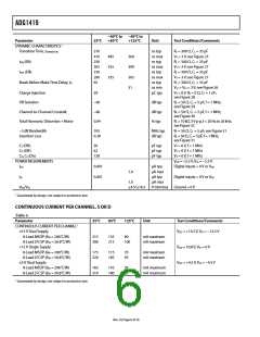
ADG1419
−40°C to
+85°C
−40°C to
+125°C
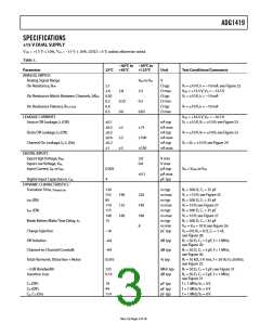
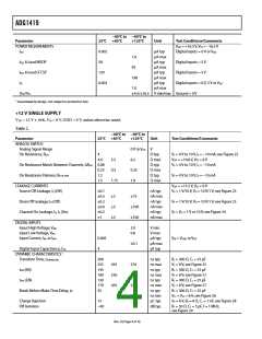
Parameter
DYNAMIC CHARACTERISTICS1
25°C
Unit
Test Conditions/Comments
Transition Time, tTRANSITION
310
410
230
305
220
290
65
ns typ
ns max
ns typ
ns max
ns typ
ns max
ns typ
ns min
pC typ
RL = 300 Ω, CL = 35 pF
VS = 3 V; see Figure 25
RL = 300 Ω, CL = 35 pF
VS = 3 V; see Figure 2±
RL = 300 Ω, CL = 35 pF
VS = 3 V; see Figure 2±
RL = 300 Ω, CL = 35 pF
VS1 = VS2 = 3 V; see Figure 26
495
355
335
560
390
365
31
tON (EN)
tOFF (EN)
Break-Before-Make Time Delay, tD
Charge Injection
59
VS = 0 V, RS = 0 Ω, CL = 1 nF;
see Figure 28
Off Isolation
−60
−60
0.04
dB typ
dB typ
% typ
RL = 50 Ω, CL = 5 pF, f = 1 MHz;
see Figure 29
RL = 50 Ω, CL = 5 pF, f = 1 MHz;
see Figure 30
RL = 10 kΩ, 5 V p-p, f = 20 Hz to 20 kHz;
see Figure 32
Channel-to-Channel Crosstalk
Total Harmonic Distortion + Noise
−3 dB Bandwidth
Insertion Loss
105
0.28
MHz typ
dB typ
RL = 50 Ω, CL = 5 pF; see Figure 31
RL = 50 Ω, CL = 5 pF, f = 1 MHz;
see Figure 31
CS (Off)
CD (Off)
CD, CS (On)
26
62
128
pF typ
pF typ
pF typ
VS = 0 V, f = 1 MHz
VS = 0 V, f = 1 MHz
VS = 0 V, f = 1 MHz
POWER REQUIREMENTS
IDD
VDD = +5.5 V, VSS = −5.5 V
Digital inputs = 0 V or VDD
0.001
0.001
μA typ
μA max
μA typ
μA max
V min/max
1.0
ISS
Digital inputs = 0 V or VDD
Ground = 0 V
1.0
±4.5/±16.5
VDD/VSS
1 Guaranteed by design, not subject to production test.
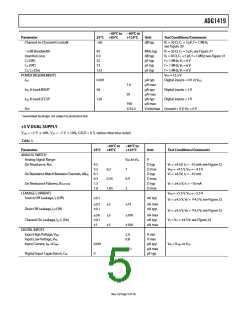
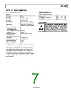
CONTINUOUS CURRENT PER CHANNEL, S OR D
Table 4.
Parameter
CONTINUOUS CURRENT PER CHANNEL1
25°C
85°C
125°C
Unit
Test Conditions/Comments
±15 V Dual Supply
VDD = +13.5 V, VSS = −13.5 V
8-Lead MSOP (θJA = 206°C/W)
8-Lead LFCSP (θJA = 50.8°C/W)
+12 V Single Supply
215
390
135
215
80
100
mA maximum
mA maximum
VDD = 10.8 V, VSS = 0 V
8-Lead MSOP (θJA = 206°C/W)
8-Lead LFCSP (θJA = 50.8°C/W)
±5 V Dual Supply
1±5
320
115
185
±0
95
mA maximum
mA maximum
VDD = +4.5 V, VSS = −4.5 V
8-Lead MSOP (θJA = 206°C/W)
8-Lead LFCSP (θJA = 50.8°C/W)
165
310
110
180
±0
95
mA maximum
mA maximum
1 Guaranteed by design, not subject to production test.
Rev. 0 | Page 6 of 16

 ADI [ ADI ]