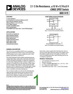
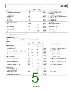
ADG1419
−40°C to −40°C to
Parameter
25°C +85°C
+125°C
Unit
Test Conditions/Comments
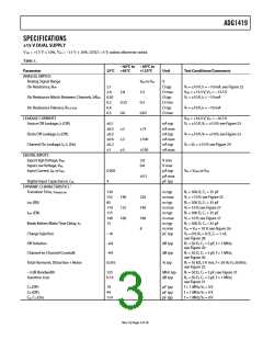
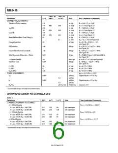
Channel-to-Channel Crosstalk
−60
dB typ
RL = 50 Ω, CL = 5 pF, f = 1 MHz;
see Figure 30
−3 dB Bandwidth
Insertion Loss
CS (Off)
CD (Off)
CD, CS (On)
95
0.3
32
±2
123
MHz typ
dB typ
pF typ
pF typ
pF typ
RL = 50 Ω, CL = 5 pF; see Figure 31
RL = 50 Ω, CL = 5 pF, f = 1 MHz; see Figure 31
f = 1 MHz; VS = 6 V
f = 1 MHz; VS = 6 V
f = 1 MHz; VS = 6 V
POWER REQUIREMENTS
IDD
VDD = 13.2 V
Digital inputs = 0 V or VDD
0.001
58
μA typ
μA max
μA typ
μA max
μA typ
μA max
1.0
95
IDD, 8-Lead MSOP
IDD, 8-Lead LFCSP
Digital inputs = 5 V
Digital inputs = 5 V
120
190
VDD
5/16.5
V min/max Ground = 0 V, VSS = 0 V
1 Guaranteed by design, not subject to production test.
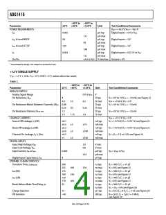
5 V DUAL SUPPLY
VDD = +5 V 10%, VSS = −5 V 10%, GND = 0 V, unless otherwise noted.
Table 3.
−40°C to
+85°C
−40°C to
+125°C
Parameter
25°C
Unit
Test Conditions/Comments
ANALOG SWITCH
Analog Signal Range
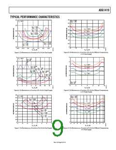
On Resistance, RON
VDD to VSS
V
4.5
5.2
Ω typ
Ω max
Ω typ
Ω max
Ω typ
Ω max
VS = ±4.5V, IS = −10 mA; see Figure 22
VDD = +4.5 V, VSS = −4.5 V
VS = ±4.5V, IS = −10 mA
6.2
±
On Resistance Match Between Channels, ∆RON 0.1
0.3
On Resistance Flatness, RFLAT (ON)
0.35
1.85
0.4
2
1.3
1.6
VS = ±4.5 V, IS = −10 mA
LEAKAGE CURRENTS
VDD = +5.5 V, VSS = −5.5 V
Source Off Leakage, IS (Off)
±0.1
nA typ
VS = ±4.5 V, VD = ∓4.5 V; see Figure 23
±0.5
±0.1
±2
±±5
nA max
nA typ
Drain Off Leakage, ID (Off)
VS = ±4.5 V, VD = ∓4.5 V; see Figure 23
±0.6
±0.1
±1
±3
±3
±100
±100
nA max
nA typ
nA max
Channel On Leakage, ID, IS (On)
VS = VD = ±4.5 V; see Figure 24
DIGITAL INPUTS
Input High Voltage, VINH
Input Low Voltage, VINL
Input Current, IINL or IINH
2.0
0.8
V min
V max
μA typ
μA max
pF typ
0.001
4
VIN = VGND or VDD
±0.1
Digital Input Capacitance, CIN
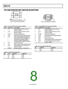
Rev. 0 | Page 5 of 16

 ADI [ ADI ]