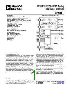
AD9888
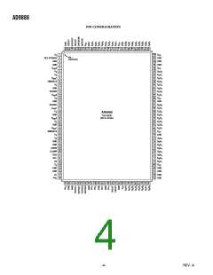
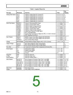
Table I. Complete Pinout List
Pin
Pin Type
Analog Video Inputs RAIN
AIN0
BAIN
RAIN
AIN1
BAIN
Mnemonic
Function
Value
Number
0
Channel 0 Analog Input for Converter R
Channel 0 Analog Input for Converter G
Channel 0 Analog Input for Converter B
Channel 1 Analog Input for Converter R
Channel 1 Analog Input for Converter G
Channel 1 Analog Input for Converter B
0.0 V to 1.0 V
0.0 V to 1.0 V 13
0.0 V to 1.0 V 20
0.0 V to 1.0 V
0.0 V to 1.0 V 17
0.0 V to 1.0 V 23
5
G
0
1
8
G
1
Sync/Clock Inputs
HSYNC0
VSYNC0
SOGIN0
HSYNC1
VSYNC1
SOGIN1
CLAMP
COAST
CKEXT
CKINV
Channel 0 Horizontal SYNC Input
Channel 0 Vertical SYNC Input
Channel 0 Input for Sync-on-Green
Channel 1 Horizontal SYNC Input
Channel 1 Vertical SYNC Input
Channel 1 Input for Sync-on-Green
Clamp Input (External CLAMP signal)
PLL Coast Signal Input
External Pixel Clock Input (to Bypass the PLL) or 10 kΩ to Ground
ADC Sampling Clock Invert
3.3 V CMOS
3.3 V CMOS
0.0 V to 1.0 V 12
3.3 V CMOS
3.3 V CMOS
0.0 V to 1.0 V 16
3.3 V CMOS
3.3 V CMOS
3.3 V CMOS
3.3 V CMOS
45
44
43
42
30
53
54
29
Sync Outputs
HSOUT
VSOUT
SOGOUT
HSYNC Output Clock (Phase-Aligned with DATACK)
VSYNC Output Clock (Phase-Aligned with DATACK)
Sync-on-Green Slicer Output
3.3 V CMOS
3.3 V CMOS
3.3 V CMOS
125
127
126
Voltage
REF BYPASS
Internal Reference Bypass (Bypass with 0.1 µF to Ground)
1.25 V 10%
2
Clamp Voltages
R
MIDSCV
Red Channel Midscale Clamp Voltage Bypass
Blue Channel Midscale Clamp Voltage Bypass
9
24
BMIDSC
V
PLL Filter
FILT
Connection for External Filter Components for Internal PLL
50
Power Supply
VD
Analog Power Supply
Output Power Supply
PLL Power Supply
Ground
3.3 V 10%
3.3 V 10%
3.3 V 10%
0 V
VDD
PVD
GND
Serial Port
(2-Wire
Serial Interface)
SDA
SCL
A0
Serial Port Data I/O
Serial Port Data Clock
Serial Port Address Input 1
3.3 V CMOS
3.3 V CMOS
3.3 V CMOS
31
32
33
Data Outputs
Red A[7:0]
Red B[7:0]
Green A[7:0]
Green B[7:0]
Blue A[7:0]
Blue B[7:0]
Port A Outputs of Converter “Red,” Bit 7 is the MSB.
Port B Outputs of Converter “Red,” Bit 7 is the MSB.
Port A Outputs of Converter “Green,” Bit 7 is the MSB.
Port B Outputs of Converter “Green,” Bit 7 is the MSB.
Port A Outputs of Converter “Blue,” Bit 7 is the MSB.
Port B Outputs of Converter “Blue,” Bit 7 is the MSB.
3.3 V CMOS
3.3 V CMOS
3.3 V CMOS
3.3 V CMOS
3.3 V CMOS
3.3 V CMOS
113–120
103–110
90–97
80–87
70–77
57–64
Data Clock
Output
DATACK
DATACK
Data Output Clock
Data Output Clock Complement
3.3 V CMOS
3.3 V CMOS
123
124
–5–
REV. A

 ADI [ ADI ]