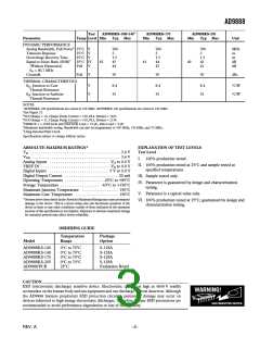
AD9888
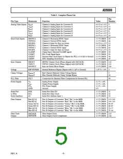
PIN FUNCTION DESCRIPTIONS (continued)
Pin
Description
Sampling Clock Inversion (Optional)
CKINV
This pin may be used to invert the pixel sampling clock, which has the effect of shifting the sampling phase 180°. This is
in support of Alternate Pixel Sampling mode, wherein higher-frequency input signals (up to 410 Mpps) may be captured by
first sampling the odd pixels, then capturing the even pixels on the subsequent frame.
This pin should be exercised only during blanking intervals (typically vertical blanking) as it may produce several
samples of corrupted data during the phase shift.
CKINV should be grounded when not used.
Outputs
DRA7-0
DRB7-0
DGA7-0
DGB7-0
DBA7-0
DBB7-0
Data Output, Red Channel, Port A
Data Output, Red Channel, Port B
Data Output, Green Channel, Port A
Data Output, Green Channel, Port B
Data Output, Blue Channel, Port A
Data Output, Blue Channel, Port B
These are the main data outputs. Bit 7 is the MSB.
Each channel has two ports. When the part is operated in single-channel mode (Channel Mode bit (15H, Bit 7) = 0), all
data are presented to Port A, and Port B is placed in a high-impedance state.
Programming the Channel Mode bit to 1 establishes dual-channel mode, wherein alternate pixels are presented to Port Aand
Port B of each channel. These will appear simultaneously; two pixels are presented at the time of every second input
pixel, when the Output Mode bit (15H, Bit 6) is set to 1 (parallel mode). When the Output Mode bit is set to 0, pixel
data appear alternately on the two ports, one new sample with each incoming pixel (interleaved mode).
In dual-channel mode, the first pixel after HSYNC is routed to Port A. The second pixel goes to Port B, the third to A,
etc. This can be reversed by setting the A/B Invert bit to 1 (15H, Bit 5).
The delay from pixel sampling time to output is fixed. When the sampling time is changed by adjusting the PHASE regis-
ter, the output timing is shifted as well. The DATACK, DATACK and HSOUT outputs are also moved, so the
timing relationship among the signals is maintained.
DATACK
Data Output Clock
DATACK
Data Output Clock Complement
Differential data clock output signals to be used to strobe the output data and HSOUT into external logic.
They are produced by the internal clock generator and are synchronous with the internal pixel sampling clock.
When the AD9888 is operated in single-channel mode, the output frequency is equal to the pixel sampling frequency.
When operating in dual-channel mode, the clock frequency is one-half the pixel frequency, as is the output data frequency.
When the sampling time is changed by adjusting the PHASE register, the output timing is shifted as well. The Data,
DATACK, DATACK and HSOUT outputs are all moved, so the timing relationship among the signals is maintained.
Either or both signals may be used, depending on the timing mode and interface design employed.
Horizontal Sync Output
HSOUT
A reconstructed and phase-aligned version of the Hsync input. Both the polarity and duration of this output can be
programmed via serial bus registers.
By maintaining alignment with DATACK, DATACK, and Data, data timing with respect to horizontal sync can always
be determined.
SOGOUT
Sync-On-Green Slicer Output
This pin can be programmed to output either the output from the Sync-On-Green slicer comparator or an unproc-
essed but delayed version of the Hsync input. See the Sync Processing Block Diagram (Figure 25) to view how this pin is
connected. (Note: Besides slicing off SOG, the output from this pin gets no other additional processing on the AD9888.
Vsync separation is performed via the sync separator.)
REF BYPASS
Internal Reference BYPASS
Bypass for the internal 1.25 V band gap reference. It should be connected to ground through a 0.1 µF capacitor. The abso-
lute accuracy of this reference is 4%, and the temperature coefficient is 50 ppm, which is adequate for most AD9888
applications. If higher accuracy is required, an external reference may be employed instead.
RMIDSCV
BMIDSCV
RED Channel Midscale Voltage BYPASS
BLUE Channel Midscale Voltage BYPASS
Bypasses for the internal midscale voltage references. They should each be connected to ground through 0.1 µF
capacitors. The exact voltage varies with the gain setting of the BLUE channel.
–7–
REV. A

 ADI [ ADI ]