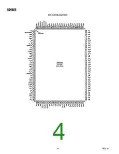
AD9888
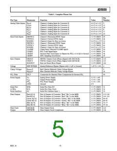
PIN FUNCTION DESCRIPTIONS (continued)
Pin
Description
FILT
External Filter Connection
For proper operation, the pixel clock generator PLL requires an external filter. Connect the filter shown in Figure 6 to this
pin. For optimal performance, minimize noise and parasitics on this node.
Power Supply
VD
Main Power Supply
These pins supply power to the main elements of the circuit. It should be as quiet and filtered as possible.
Digital Output Power Supply
VDD
A large number of output pins (up to 52) switching at high speed (up to 110 MHz) generates a lot of power supply
transients (noise). These supply pins are identified separately from the VD pins, so special care can be taken to mini-
mize output noise transferred into the sensitive analog circuitry. If the AD9888 is interfacing with lower voltage logic,
V
DD may be connected to a lower supply voltage (as low as 2.5 V) for compatibility.
PVD
Clock Generator Power Supply
The most sensitive portion of the AD9888 is the clock generation circuitry. These pins provide power to the clock PLL
and help the user design for optimal performance. The designer should provide “quiet,” noise-free power to these pins.
GND
Ground
The ground return for all circuitry on chip. It is recommended that the AD9888 be assembled on a single solid ground plane,
with careful attention to ground current paths.
Serial Port (2-Wire)
SDA
SCL
A0
Serial Port Data I/O
ISerial Port Data Clock
Serial Port Address Input 1
For a full description of the 2-wire serial register and how it works, refer to the Control Register section.
DESIGN GUIDE
At that point, the signal should be resistively terminated (to the
General Description
signal ground return) and capacitively coupled to the AD9888
inputs through 47 nF capacitors. These capacitors form part of
the dc restoration circuit.
The AD9888 is a fully integrated solution for capturing analog
RGB signals and digitizing them for display on flat panel monitors
or projectors. The circuit is ideal for providing a computer inter-
face for HDTV monitors or as the front-end to high-performance
video scan converters.
In an ideal world of perfectly matched impedances, the best
performance can be obtained with the widest possible signal
bandwidth. The ultrawide bandwidth inputs of the AD9888
(500 MHz) can track the input signal continuously as it moves
from one pixel level to the next, and digitize the pixel during
a long, flat pixel time. In many systems, however, there are
mismatches, reflections, and noise, which can result in excessive
ringing and distortion of the input waveform. This makes it
more difficult to establish a sampling phase that provides good
image quality. The AD9888 can digitize graphics signals over a
very wide range of frequencies (10 MHz to 205 MHz). Often
characteristics that are beneficial at one frequency can be detri-
mental at another. Analog bandwidth is one such characteristic.
For UXGA resolutions (up to 205 MHz), a very high analog
bandwidth is desirable because of the fast input signal slew
rates. For VGA and lower resolutions (down to 12.5 MHz), a
very high bandwidth is not desirable, because it allows excess
noise to pass through. To accommodate these varying needs,
the AD9888 includes variable analog bandwidth control.
Four settings are available (75 MHz, 150 MHz, 300 MHz,
and 500 MHz), allowing the analog bandwidth to be matched
with the resolution of the incoming graphics signal.
Implemented in a high-performance CMOS process, the inter-
face can capture signals with pixel rates of up to 205 MHz, and
with an Alternate Pixel Sampling mode, up to 340 MHz.
The AD9888 includes all necessary input buffering, signal dc
restoration (clamping), offset and gain (brightness and contrast)
adjustment, pixel clock generation, sampling phase control, and
output data formatting. All controls are programmable via a
2-wire serial interface. Full integration of these sensitive analog
functions makes system design straightforward and less sensitive
to the physical and electrical environment.
With a typical power dissipation of only 650 mW and an operat-
ing temperature range of 0°C to 70°C, the device requires no
special environmental considerations.
Input Signal Handling
The AD9888 has six high-impedance analog input pins for the
red, green, and blue channels. They will accommodate signals
ranging from 0.5 V to 1.0 V p-p.
Signals are typically brought onto the interface board via a DVI-I
connector, a 15-pin D connector, or via BNC connectors. The
AD9888 should be located as close as practical to the input
connector. Signals should be routed via matched-impedance
traces (normally 75 Ω) to the IC input pins.
47nF
R
AIN
AIN
RGB
INPUT
G
B
AIN
75⍀
Figure 1. Analog Input Interface Circuit
–8–
REV. A

 ADI [ ADI ]