AD9888
Test
Temp Level Min
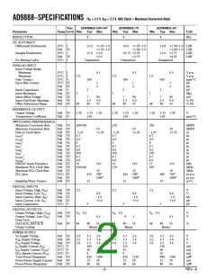
AD9888KS-100/-1401
AD9888KS-170
AD9888KS-205
Parameter
Typ
Max
Min
Typ
Max
Min
Typ
Max
Unit
DYNAMIC PERFORMANCE
Analog Bandwidth, Full Power6 25°C
V
V
V
500
2
1.5
45
44
500
2
1.5
44
43
500
2
1.5
42
41
MHz
ns
ns
dB
dB
Transient Response
Overvoltage Recovery Time
Signal-to-Noise Ratio (SNR)7
(Without Harmonics)
fIN = 40.7 MHz
25°C
25°C
25°C IV
42
41
40
Full
V
Crosstalk
Full
V
50
50
50
dBc
THERMAL CHARACTERISTICS
θ
JC–Junction-to-Case
Thermal Resistance
JA–Junction-to-Ambient
Thermal Resistance
V
V
8.4
35
8.4
35
8.4
35
°C/W
°C/W
θ
NOTES
1AD9888KS-100 specifications are tested at 100 MHz. AD9888KS-140 specifications are tested at 140 MHz.
2See Figure 23.
3VCO Range = 10, Charge Pump Current = 100, PLL Divider = 1693.
4VCO Range = 11, Charge Pump Current = 100, PLL Divider = 2159.
5DEMUX = 1, DATACK and DATACK Load = 15 pF, Data Load = 5 pF.
6Maximum bandwidth setting. Bandwidth can also be programmed to 300 MHz, 150 MHz, and 75 MHz.
7Using External Pixel Clock.
Specifications subject to change without notice.
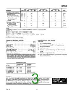
ABSOLUTE MAXIMUM RATINGS*
EXPLANATION OF TEST LEVELS
Test Level
VD . . . . . . . . . . . . . . . . . . . . . . . . . . . . . . . . . . . . . . . . . . 3.6 V
VDD . . . . . . . . . . . . . . . . . . . . . . . . . . . . . . . . . . . . . . . . . 3.6 V
Analog Inputs . . . . . . . . . . . . . . . . . . . . . . . . . . . . VD to 0.0 V
VREF IN . . . . . . . . . . . . . . . . . . . . . . . . . . . . . . . . VD to 0.0 V
Digital Inputs . . . . . . . . . . . . . . . . . . . . . . . . . . . 5 V to 0.0 V
Digital Output Current . . . . . . . . . . . . . . . . . . . . . . . . . 20 mA
Operating Temperature . . . . . . . . . . . . . . . . . –25°C to +85°C
Storage Temperature . . . . . . . . . . . . . . . . . . –65°C to +150°C
Maximum Junction Temperature . . . . . . . . . . . . . . . . . 150°C
Maximum Case Temperature . . . . . . . . . . . . . . . . . . . . 150°C
I. 100% production tested.
II. 100% production tested at 25°C and sample tested at
specified temperatures.
III. Sample tested only.
IV. Parameter is guaranteed by design and characterization
testing.
V. Parameter is a typical value only.
*Stresses above those listed under Absolute Maximum Ratings may cause permanent
damage to the device. This is a stress rating only and functional operation of the
device at these or any other conditions outside of those indicated in the operation
sections of this specification is not implied. Exposure to absolute maximum ratings
for extended periods may affect device reliability.
VI. 100% production tested at 25°C; guaranteed by design and
characterization testing.
ORDERING GUIDE
Temperature
Range
Package
Option
Model
AD9888KS-100
AD9888KS-140
AD9888KS-170
AD9888KS-205
AD9888/PCB
0°C to 70°C
0°C to 70°C
0°C to 70°C
0°C to 70°C
25°C
S-128A
S-128A
S-128A
S-128A
Evaluation Board
CAUTION
ESD (electrostatic discharge) sensitive device. Electrostatic charges as high as 4000 V readily
accumulate on the human body and test equipment and can discharge without detection. Although
the AD9888 features proprietary ESD protection circuitry, permanent damage may occur on
devices subjected to high-energy electrostatic discharges. Therefore, proper ESD precautions are
recommended to avoid performance degradation or loss of functionality.
WARNING!
ESD SENSITIVE DEVICE
–3–
REV. A

 ADI [ ADI ]