AD9807/AD9805
ABSO LUTE MAXIMUM RATINGS*
D EFINITIO NS O F SP ECIFICATIO NS
INTEGRAL NO NLINEARITY
With
Linearity error refers to the deviation of each individual code
from a line drawn from “negative full scale” through “positive
full scale.” The point used as “negative full scale” occurs 1/2 LSB
before the first code transition. “Positive full scale” is defined as a
level 1 1/2 LSB beyond the last code transition. T he deviation is
measured from the middle of each particular code to the true
straight line.
Respect
to
P aram eter
Min Max
Units
AVDD
AVSS
DVDD
AGND
AVSS
AVDD
DVSS
DVSS
DVDD
DVSS
DVSS
AVSS
–0.5 +6.5
–6.5 +0.5
–0.5 +6.5
–0.3 +0.3
–6.5 +6.5
–0.5 DVDD + 0.5 Volts
–0.5 AVDD + 0.3 Volts
–0.3 AVDD + 0.3 Volts
Volts
Volts
Volts
Volts
Volts
AVDD
D IFFERENTIAL LINEARITY ERRO R (D NL, NO MISSING
CO D ES)
Clock Input
Digital Outputs
AIN, VREF
Junction T emperature
Storage T emperature
An ideal ADC exhibits code transitions that are exactly 1 LSB
apart. DNL is the deviation from this ideal value. T hus every
code must have a finite width. Guaranteed no missing codes
to 12-bit resolution indicates that all 4096 codes, respectively,
must be present over all operating ranges.
+150
–65 +150
+300
°C
°C
°C
Lead T emperature (10 sec)
*Stresses above those listed under “Absolute Maximum Ratings” may cause
permanent damage to the device. T his is a stress rating only; functional operation
of the device at these or any other conditions above those indicated in the
operational sections of this specification is not implied. Exposure to absolute
maximum ratings for extended periods may affect device reliability.
UNIP O LAR O FFSET ERRO R
In the unipolar mode, the first transition should occur at a level
1/2 LSB above analog common. Unipolar offset is defined as
the deviation of the actual from that point. T he unipolar offset
temperature coefficient specifies the maximum change of the
transition point over temperature, with or without external
adjustments.
O RD ERING GUID E
Tem perature
Range
P ackage
D escription
P ackage
O ption*
Model
AD9807JS
AD9805JS
0°C to +70°C
0°C to +70°C
PQFP
PQFP
S-64
S-64
GAIN ERRO R
T he last transition should occur for an analog value 1 1/2 LSB
below the nominal full scale. Gain error is the deviation of the
actual difference between first and last code transitions and the
ideal difference between first and last code transitions.
*S = Plastic Quad Flatpack.
P O WER SUP P LY REJECTIO N
Power Supply Rejection specifies the maximum full-scale change
from the initial value with the supplies at the various limits.
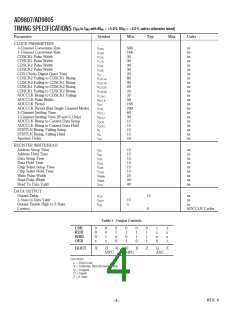
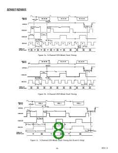
AP ERTURE D ELAY
Aperture delay is a timing measurement between the sampling
clocks and the CDS. It is measured from the falling edge of the
CDSCLK2 input to when the input signal is held for conversion
in CDS mode. In non-CDS mode, it is the falling edge of
CDSCLK1.
CAUTIO N
ESD (electrostatic discharge) sensitive device. Electrostatic charges as high as 4000 V readily
accumulate on the human body and test equipment and can discharge without detection.
Although the AD9807/AD9805 feature proprietary ESD protection circuitry, permanent damage
may occur on devices subjected to high energy electrostatic discharges. T herefore, proper ESD
precautions are recommended to avoid performance degradation or loss of functionality.
WARNING!
ESD SENSITIVE DEVICE
REV. 0
–7–

 ADI [ ADI ]