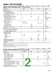
AD9807–SPECIFICATIONS
MAX with AV = +5.0 V, DV = +5.0 V, fADCCLK = 6 MSPS, fCDSCLK1 = 2 MSPS, fCDSCLK2 = 2 MSPS,
PGA Gain = 1 unless otherwise noted)
ANALOG SPECIFICATIONS (T to T
MIN
DD
DD
P aram eter
Min
Typ
Max
Units
RESOLUT ION
12
Bits
CONVERSION RAT E
3-Channel Mode With CDS
6
6
MSPS
MSPS
1-Channel Mode With CDS1
DC ACCURACY
Integral Nonlinearity (INL)2
Differential Nonlinearity (DNL)2
No Missing Codes
1.5
0.4
LSB
LSB
Bits Guaranteed
% FSR
% FSR
0.75
12
Unipolar Offset Error (@ +25°C)
Gain Error (@ +25°C)
0.4
1.2
ANALOG INPUT S
Full-Scale Input Span
Input Limits3
0.0625
AVSS – 0.3 V
4
V p-p
V
AVDD + 0.3
Input Capacitance
Input Bias Current
Input Referred Noise
10
0.01
0.3
pF
µA
LSB rms
PSRR (AVDD = +5 V ± 0.25 V)
0.06
% FSR
INT ERNAL VOLT AGE REFERENCE
1 V Output T olerance (@+25°C)
2 V Output T olerance (@+25°C)
±15
±30
mV
mV
POWER SUPPLIES
Operating Voltages
AVDD
+4.75
+4.75
+5.25
+5.25
V
V
DVDD
Operating Current
AVDD
DVDD
73
16.6
86
20
mA
mA
POWER CONSUMPT ION
450
530
mW
T EMPERAT URE RANGE
Operating
0
+70
°C
NOT ES
1Blue and green channels. Red channel conversion rate for 1-channel mode is 5 MSPS.
2Measured with 4 V p-p input range.
3Input signals exceeding these limits are subject to excessive overvoltage recovery times.
Specifications subject to change without notice.
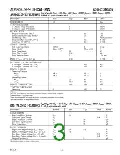
(TMIN to TMAX with AV = +5.0 V, DV = +5.0 V, fADCCLK = 6 MSPS, fCDSCLK1 = 2 MSPS, fCDSCLK2 = 2 MSPS,
DD
DD
DIGITAL SPECIFICATIONS
P aram eter
C = 20 pF, unless otherwise noted)
L
Sym bol
Min
Typ
Max
Units
LOGIC INPUT S
High Level Input Voltage
Low Level Input Voltage
High Level Input Current
Low Level Input Current
Input Capacitance
VIH
VIL
IIH
IIL
CIN
2.0
V
V
µA
µA
pF
0.8
10
10
10
LOGIC OUT PUT S
High Level Output Voltage (IOH = 50 µA)
High Level Output Voltage (IOH = 0.5 mA)
Low Level Output Voltage (IOL = 50 µA)
Low Level Output Voltage (IOL = –0.6 mA)
Output Capacitance
VOH
VOH
VOL
VOL
COUT
4.5
2.4
4.9
5
V
V
V
V
0.1
0.4
pF
Specifications subject to change without notice.
REV. 0
–2–

 ADI [ ADI ]