AD9807/AD9805
CIS Application
CIS START PULSE
CIS CLOCK
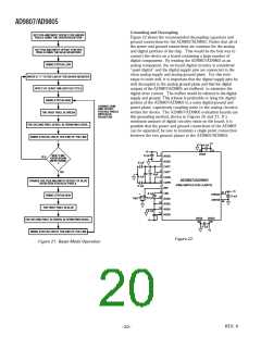
Unlike many other integrated circuit CCD signal processors, the
AD9807/AD9805 can easily be implemented in imaging systems
that do not use a CCD. By disabling the input clamp and the
CDS blocks, any dc coupled signal within the input limits of the
part can be digitized. Figure 23 shows a typical block diagram of
the AD9807 used with a color CIS module, in this case Dyna
Image Corporation’s DL100*. T he three color output signals
are dc coupled into the AD9807. T he Dyna CIS module’s
output levels are around 70 mV to 500 mV dark to bright, well
within the input range of the AD9807. T he AD9807 is config-
ured for 3-channel SHA operation through the MPU registers.
Timing used with the Dyna DL100 is shown in Figure 24; the
CIS output levels are sampled on the falling edge of CDSCLK1.
T he digital ASIC shown can be implemented in a variety of
ways: it could include the MPU interface and timing generator,
as well as memory for the output data and pixel gain and offset
correction vectors.
CIS OUTPUT
STRTLN
ADCCLK
CDSCLK1
Figure 24. CIS Application Tim ing Signals
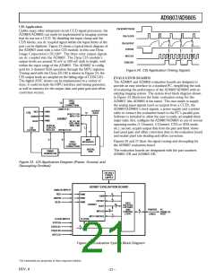
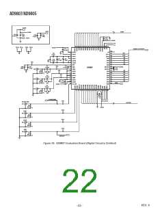
EVALUATIO N BO ARD S
T he AD9807 and AD9805 evaluation boards are designed to
provide an easy interface to a standard PC, simplifying the task
of evaluating the performance of the AD9807/AD9805 with an
existing imaging system. T he system level block diagram shown
in Figure 25 illustrates the basic evaluation setup for the
AD9807 (the AD9805 is the same). T he user needs to supply
the analog input signals (such as outputs from a CCD), the
AD9807/AD9805’s clock signals, a power supply and a printer
cable to connect the evaluation board to the PC’s parallel port.
Software is included to allow the user to easily accomplish three
major tasks: first, configure the AD9807/AD9805 in one of several
operating modes (1 Channel, 3 Channel, CDS or SHA mode,
etc.), second, acquire output data from the part and third, down-
load pixel gain and offset correction data to the evaluation board
and enable pixel rate shading and offset correction.
PIXEL
GAIN
CORRECTION
12
GAIN<11:0>
DOUT<11:0>
OUTPUT
DATA
VINR
VING
VINB
RED
GREEN
BLUE
CIS
12
MPU<7:0>
AD9807
A2, A1, A0
OEB, WRB
RDB, CSB
STRTLN,
CDSCLK1,
ADCCLK
CIS
CLOCKS
7
OFFSET<7:0>
8
3
8
MPU
Figures 26 and 27 show the signal routing and decoupling for
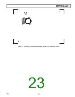
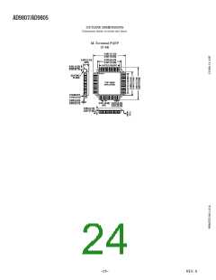
the AD9807 evaluation board.
INTERFACE
PIXEL
OFFSET
CORRECTION
DIGITAL
ASIC
T he evaluation boards are designated with the part numbers
AD9807-EB and AD9805-EB.
TIMING
GENERATOR
Figure 23. CIS Application Diagram (Power, Ground, and
Decoupling Om itted)
+5V VOLT
POWER
SUPPLY
AD9807 EVALUATION BOARD
ANALOG INPUTS
RED
12
VINR
VING
VINB
GAIN
GREEN
8
OFFSET
BLUE
FIFO
AD9807
12
BUFFERS,
LATCHES,
AND
CONTROL
LOGIC
DOUT
8
PRINTER
CABLE
PC
PARALLEL
PORT
8
MPU I/O
7
MPU CONTROL
CLOCK INPUTS
STRTLN
CLOCKS
4
CDSCLK1
CDSCLK2
ADCCLK
Figure 25. Evaluation System Block Diagram
*All trademarks are properties of their respective holders.
REV. 0
–21–

 ADI [ ADI ]