AD9653
Data Sheet
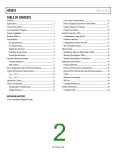
TABLE OF CONTENTS
Features .............................................................................................. 1
Clock Input Considerations...................................................... 25
Power Dissipation and Power-Down Mode ........................... 27
Digital Outputs and Timing ..................................................... 27
Output Test Modes..................................................................... 30
Serial Port Interface (SPI).............................................................. 31
Configuration Using the SPI..................................................... 31
Hardware Interface..................................................................... 32
Configuration Without the SPI ................................................ 32
SPI Accessible Features.............................................................. 32
Memory Map .................................................................................. 33
Reading the Memory Map Register Table............................... 33
Memory Map Register Table..................................................... 34
Memory Map Register Descriptions........................................ 37
Applications Information .............................................................. 39
Design Guidelines ...................................................................... 39
Power and Ground Recommendations ................................... 39
Exposed Pad Thermal Heat Slug Recommendations............ 39
VCM............................................................................................. 39
Reference Decoupling................................................................ 39
SPI Port ........................................................................................ 39
Crosstalk Performance .............................................................. 39
Outline Dimensions ....................................................................... 40
Ordering Guide .......................................................................... 40
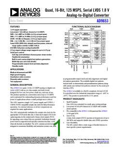
Applications....................................................................................... 1
General Description ......................................................................... 1
Functional Block Diagram .............................................................. 1
Product Highlights ........................................................................... 1
Revision History ............................................................................... 2
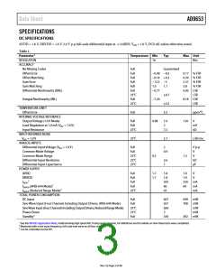
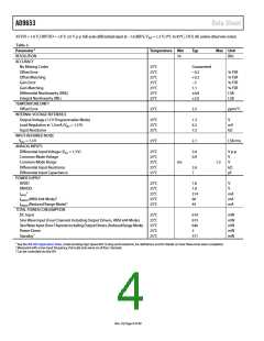
Specifications..................................................................................... 3
DC Specifications ......................................................................... 3
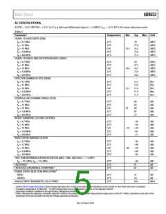
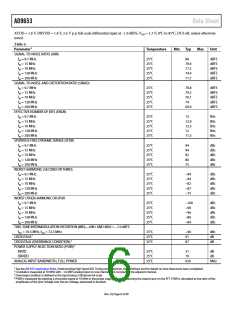
AC Specifications.......................................................................... 5
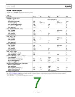
Digital Specifications ................................................................... 7
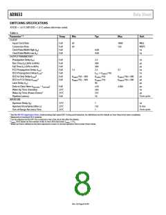
Switching Specifications .............................................................. 8
Timing Specifications .................................................................. 9
Absolute Maximum Ratings.......................................................... 11
Thermal Resistance .................................................................... 11
ESD Caution................................................................................ 11
Pin Configuration and Function Descriptions........................... 12
Typical Performance Characteristics ........................................... 14
VREF = 1.0 V ................................................................................. 14
VREF = 1.3 V ................................................................................. 17
Equivalent Circuits ......................................................................... 21
Theory of Operation ...................................................................... 22
Analog Input Considerations.................................................... 22
Voltage Reference ....................................................................... 23
REVISION HISTORY
5/12—Revision 0: Initial Version
Rev. 0 | Page 2 of 40

 ADI [ ADI ]