AD9268
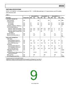
PIN CONFIGURATIONS AND FUNCTION DESCRIPTIONS
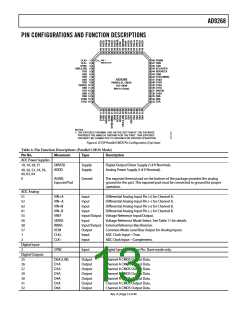
PIN 1
INDICATOR
CLK+
CLK–
SYNC
D0B (LSB)
D1B
D2B
D3B
D4B
D5B
DRVDD 10
D6B 11
D7B 12
D8B 13
D9B 14
1
2
3
4
5
6
7
8
9
48 PDWN
47 OEB
46 CSB
45 SCLK/DFS
44 SDIO/DCS
43 ORA
42 D15A (MSB)
41 D14A
40 D13A
39 D12A
38 D11A
AD9268
PARALLEL CMOS
TOP VIEW
(Not to Scale)
37 DRVDD
36 D10A
35 D9A
D10B 15
D11B 16
34 D8A
33 D7A
NOTES
1. THE EXPOSED THERMAL PAD ON THE BOTTOM OF THE PACKAGE
PROVIDES THE ANALOG GROUND FOR THE PART. THIS EXPOSED
PAD MUST BE CONNECTED TO GROUND FOR PROPER OPERATION.
Figure 6. LFCSP Parallel CMOS Pin Configuration (Top View)
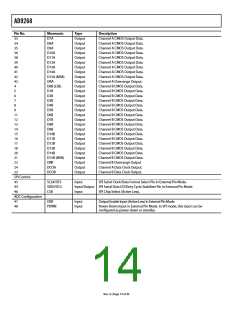
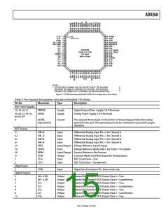
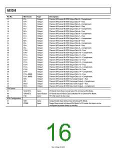
Table 8. Pin Function Descriptions (Parallel CMOS Mode)
Pin No.
Mnemonic
Type
Description
ADC Power Supplies
1±, 19, 28, 3ꢁ
49, ꢀ±, ꢀ3, ꢀ4, ꢀ9,
6±, 63, 64
DRVDD
AVDD
Supply
Supply
Digital Output Driver Supply (1.8 V Nominal).
Analog Power Supply (1.8 V Nominal).
±
AGND,
Exposed Pad
Ground
The exposed thermal pad on the bottom of the package provides the analog
ground for the part. This exposed pad must be connected to ground for proper
operation.
ADC Analog
ꢀ1
ꢀ2
62
61
VIN+A
VIN−A
VIN+B
VIN−B
VREF
Input
Input
Input
Input
Differential Analog Input Pin (+) for Channel A.
Differential Analog Input Pin (−) for Channel A.
Differential Analog Input Pin (+) for Channel B.
Differential Analog Input Pin (−) for Channel B.
ꢀꢀ
Input/Output Voltage Reference Input/Output.
ꢀ6
ꢀ8
ꢀꢁ
1
SENSE
RBIAS
VCM
CLK+
CLK−
Input
Voltage Reference Mode Select. See Table 11 for details.
Input/Output External Reference Bias Resistor.
Output
Input
Common-Mode Level Bias Output for Analog Inputs.
ADC Clock Input—True.
ADC Clock Input—Complement.
2
Input
Digital Input
3
SYNC
Input
Digital Synchronization Pin. Slave mode only.
Digital Outputs
2ꢀ
26
2ꢁ
29
3±
31
32
D±A (LSB)
D1A
D2A
D3A
D4A
Output
Output
Output
Output
Output
Output
Output
Channel A CMOS Output Data.
Channel A CMOS Output Data.
Channel A CMOS Output Data.
Channel A CMOS Output Data.
Channel A CMOS Output Data.
Channel A CMOS Output Data.
Channel A CMOS Output Data.
DꢀA
D6A
Rev. A | Page 13 of 44

 ADI [ ADI ]