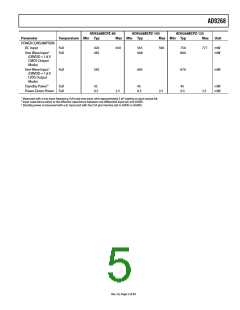
AD9268
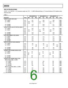
SWITCHING SPECIFICATIONS
AVDD = 1.8 V, DRVDD = 1.8 V, maximum sample rate, VIN = −1.0 dBFS differential input, 1.0 V internal reference, and DCS enabled,
unless otherwise noted.
Table 4.
AD9268BCPZ-80
Temperature Min Typ Max Min Typ
AD9268BCPZ-105
AD9268BCPZ-125
Max Unit
Parameter
Max Min Typ
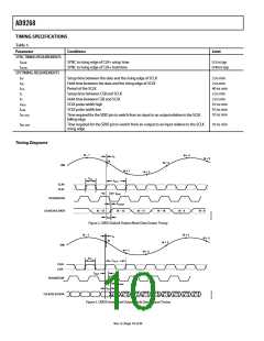
CLOCK INPUT PARAMETERS
Input Clock Rate
Conversion Rate1
DCS Enabled
DCS Disabled
CLK Period—Divide-by-1 Mode (tCLK
Full
625
625
625
MHz
Full
Full
Full
20
10
12.5
80
80
20
10
9.5
105
105
20
10
8
125
125
MSPS
MSPS
ns
)
CLK Pulse Width High (tCH)
3.75
5.95
0.8
8.75
6.55
2.85
4.5
6.65
5.0
Divide-by-1 Mode, DCS Enabled
Divide-by-1 Mode, DCS Disabled
Divide-by-2 Mode Through Divide- Full
by-8 Mode
Full
Full
6.25
6.25
4.75
4.75
2.4
3.8
0.8
4
4
5.6
4.2
ns
ns
ns
0.8
Aperture Delay (tA)
Aperture Uncertainty (Jitter, tJ)
Full
Full
1.0
0.07
1.0
0.07
1.0
0.07
ns
ps
rms
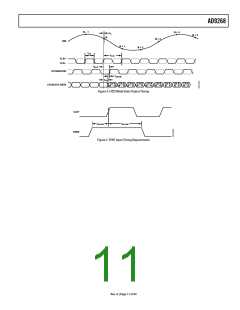
DATA OUTPUT PARAMETERS
CMOS Mode
2.8
4.2
0
2.8
4.2
0
Data Propagation Delay (tPD)
DCO Propagation Delay (tDCO
Full
Full
Full
3.5
3.1
3.5
3.1
2.8
3.5
3.1
4.2
0
ns
ns
ns
2
)
DCO to Data Skew (tSKEW
LVDS Mode
)
−0.6 −0.4
−0.6 −0.4
−0.6 −0.4
Data Propagation Delay (tPD)
DCO Propagation Delay (tDCO
Full
Full
Full
Full
2.9
3.7
3.9
4.5
2.9
3.7
3.9
4.5
2.9
3.7
3.9
4.5
ns
ns
2
)
DCO to Data Skew (tSKEW
)
−0.1 +0.2
12
+0.5 −0.1 +0.2
12
+0.5 −0.1 +0.2
12
+0.5 ns
Cycles
CMOS Mode Pipeline Delay
(Latency)
LVDS Mode Pipeline Delay (Latency) Full
Channel A/Channel B
12/12.5
12/12.5
12/12.5
Cycles
Wake-Up Time3
Full
Full
500
2
500
2
500
2
μs
Cycles
Out-of-Range Recovery Time
1 Conversion rate is the clock rate after the divider.
2 Additional DCO delay can be added by writing to Bit 0 through Bit 4 in SPI Register 0x17 (see Table 17).
3 Wake-up time is defined as the time required to return to normal operation from power-down mode.
Rev. A | Page 9 of 44

 ADI [ ADI ]