AD8325
APPLICATIONS
General Application
with a transformer, the stated gain values already take into account
the losses associated with the transformer.
The AD8325 is primarily intended for use as the upstream
power amplifier (PA) in DOCSIS (Data Over Cable Service
Interface Specifications) certified cable modems and CATV
set-top boxes. Upstream data is modulated in QPSK or QAM
format, and done with DSP or a dedicated QPSK/QAM modula-
tor. The amplifier receives its input signal from the QPSK/QAM
modulator or from a DAC. In either case the signal must be
low-pass filtered before being applied to the amplifier. Because
the distance from the cable modem to the central office will vary
with each subscriber, the AD8325 must be capable of varying its
output power by applying gain or attenuation to ensure that all
signals arriving at the central office are of the same amplitude.
The upstream signal path contains components such as a trans-
former and diplexer that will result in some amount of power loss.
Therefore, the amplifier must be capable of providing enough
power into a 75 Ω load to overcome these losses without sacri-
ficing the integrity of the output signal.
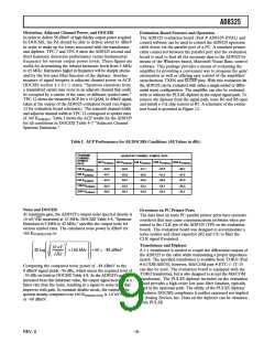
The gain transfer function is as follows:
AV = 30.0 dB – (0.7526 dB × (79 – CODE)) for 0 ≤ CODE ≤ 79
where AV is the gain in dB and CODE is the decimal equivalent
of the 8-bit word.
Valid gain codes are from 0 to 79. Figure 4 shows the gain char-
acteristics of the AD8325 for all possible values in an 8-bit
word. Note that maximum gain is achieved at Code 79. From
Code 80 through 127, the 5.25 dB of attenuation from the ver-
nier stage is being applied over every eight codes, resulting in
the sawtooth characteristic at the top of the gain range. Because
the eighth bit is a “don’t care” bit, the characteristic for codes 0
through 127 repeats from Codes 128 through 255.
30
25
20
15
Operational Description
The AD8325 is composed of four analog functions in the power-
up or forward mode. The input amplifier (preamp) can be used
single-endedly or differentially. If the input is used in the differ-
ential configuration, it is imperative that the input signals are 180
degrees out of phase and of equal amplitudes. This will ensure
proper gain accuracy and harmonic performance. The preamp
stage drives a vernier stage that provides the fine tune gain
adjustment. The 0.7526 dB step resolution is implemented in
the vernier stage and provides a total of approximately 5.25 dB of
attenuation. After the vernier stage, a DAC provides the bulk
of the AD8325’s attenuation (9 bits or 54 dB). The signals in the
preamp and vernier gain blocks are differential to improve the
PSRR and linearity. A differential current is fed from the DAC
into the output stage, which amplifies these currents to the
appropriate levels necessary to drive a 75 Ω load. The output
stage utilizes negative feedback to implement a differential
75 Ω output impedance. This eliminates the need for external
matching resistors needed in typical video (or video filter) ter-
mination requirements.
10
5
0
–5
–10
–15
–20
–25
–30
0
32
64
96
128
160
192
224
256
GAIN CODE – Decimal
Figure 4. Gain vs. Gain Code
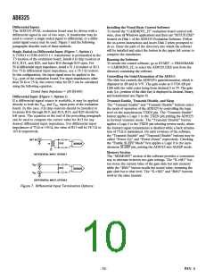
Input Bias, Impedance, and Termination
The VIN+ and VIN– inputs have a dc bias level of approximately
CC/2, therefore the input signal should be ac-coupled. The
differential input impedance is approximately 1600 Ω while the
single-ended input impedance is 800 Ω. If the AD8325 is being
operated in a single-ended input configuration with a desired
input impedance of 75 Ω, the VIN+ and VIN– inputs should be
terminated as shown in Figure 5. If an input impedance other
than 75 Ω is desired, the values of R1 and R2 in Figure 5 can be
calculated using the following equations:
V
SPI Programming and Gain Adjustment
Gain programming of the AD8325 is accomplished using a
serial peripheral interface (SPI) and three digital control lines,
DATEN, SDATA, and CLK. To change the gain, eight bits
of data are streamed into the serial shift register through the
SDATA port. The SDATA load sequence begins with a falling
edge on the DATEN pin, thus activating the CLK line. With the
CLK line activated, data on the SDATA line is clocked into the
serial shift register Most Significant Bit (MSB) first, on the rising
edge of each CLK pulse. Because only a 7-bit shift register is
used, the MSB of the 8-bit word is a “don’t care” bit and is shifted
out of the register on the eighth clock pulse. A rising edge on
the DATEN line latches the contents of the shift register into
the attenuator core resulting in a well controlled change in the
output signal level. The serial interface timing for the AD8325 is
shown in Figures 2 and 3. The programmable gain range of the
AD8325 is –29.45 dB to +30 dB and scales 0.7526 dB per least
significant bit (LSB). Because the AD8325 was characterized
ZIN = R1ꢀ800
R2 = ZINꢀR1
Z
= 75⍀
IN
–
AD8325
R1 = 82.5⍀
+
R2 = 39.2⍀
Figure 5. Single-Ended Input Termination
REV. 0
–7–

 ADI [ ADI ]