AD8325
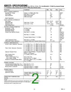
ABSOLUTE MAXIMUM RATINGS*
Supply Voltage +VS
Pins 5, 9, 10, 19, 20, 23, 27 . . . . . . . . . . . . . . . . . . . . . . 6 V
Input Voltages
Pins 25, 26 . . . . . . . . . . . . . . . . . . . . . . . . . . . . . . . .
Pins 1, 2, 3, 6, 7 . . . . . . . . . . . . . . . . . . . . . –0.8 V to +5.5 V
Internal Power Dissipation
TSSOP . . . . . . . . . . . . . . . . . . . . . . . . . . . . . . . . . . . 0.9 W
Operating Temperature Range . . . . . . . . . . . –40°C to +85°C
Storage Temperature Range . . . . . . . . . . . . –65°C to +150°C
Lead Temperature, Soldering 60 seconds . . . . . . . . . . . 300°C
*Stresses above those listed under Absolute Maximum Ratings may cause perma-
nent damage to the device. This is a stress rating only; functional operation of the
device at these or any other conditions above those indicated in the operational
section of this specification is not implied. Exposure to absolute maximum rating
conditions for extended periods may affect device reliability.
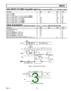
PIN CONFIGURATION
1
2
GND
28
27
26
25
24
23
22
21
20
19
18
17
16
15
DATEN
SDATA
CLK
V
CC
3
V
0.5 V
IN–
GND
4
V
IN+
V
5
GND
CC
TXEN
6
V
CC
AD8325
TOP VIEW
(Not to Scale)
7
GND
BYP
SLEEP
GND
8
V
9
V
CC
CC
V
10
V
CC
CC
GND 11
GND 12
GND 13
OUT– 14
GND
GND
GND
OUT+
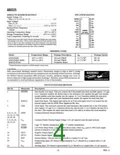
ORDERING GUIDE
Model
Temperature Range
Package Description
JA
Package Option
AD8325ARU
AD8325ARU-REEL
AD8325-EVAL
–40°C to +85°C
–40°C to +85°C
28-Lead TSSOP
28-Lead TSSOP
Evaluation Board
67.7°C/W*
67.7°C/W*
RU-28
RU-28
*Thermal Resistance measured on SEMI standard 4-layer board.
CAUTION
ESD (electrostatic discharge) sensitive device. Electrostatic charges as high as 4000 V readily
accumulate on the human body and test equipment and can discharge without detection. Although
the AD8325 features proprietary ESD protection circuitry, permanent damage may occur on
devices subjected to high-energy electrostatic discharges. Therefore, proper ESD precautions are
recommended to avoid performance degradation or loss of functionality.
WARNING!
ESD SENSITIVE DEVICE
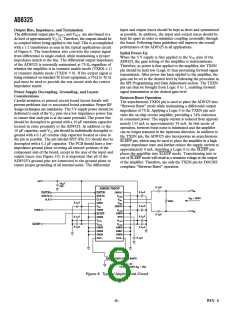
PIN FUNCTION DESCRIPTIONS
Pin No.
Mnemonic
Description
1
DATEN
Data Enable Low Input. This port controls the 8-bit parallel data latch and shift register. A Logic
0-to-1 transition transfers the latched data to the attenuator core (updates the gain) and simulta-
neously inhibits serial data transfer into the register. A 1-to-0 transition inhibits the data latch
(holds the previous gain state) and simultaneously enables the register for serial data load.
2
3
SDATA
CLK
Serial Data Input. This digital input allows for an 8-bit serial (gain) word to be loaded into the
internal register with the MSB (Most Significant Bit) first.
Clock Input. The clock port controls the serial attenuator data transfer rate to the 8-bit master-
slave register. A Logic 0-to-1 transition latches the data bit and a 1-to-0 transfers the data bit to
the slave. This requires the input serial data word to be valid at or before this clock transition.
4, 8, 11, 12,
13, 16, 17, 18,
22, 24, 28
GND
VCC
Common External Ground Reference.
5, 9, 10, 19,
20, 23, 27
Common Positive External Supply Voltage. A 0.1 µF capacitor must decouple each pin.
6
7
TXEN
Logic “0” disables transmission. Logic “1” enables transmission.
SLEEP
Low Power Sleep Mode. Logic 0 enables Sleep mode, where ZOUT goes to 400 Ω and supply
current is reduced to 4 mA. Logic 1 enables normal operation.
14
15
21
25
OUT–
OUT+
BYP
Negative Output Signal.
Positive Output Signal.
Internal Bypass. This pin must be externally ac-coupled (0.1 µF cap).
Noninverting Input. DC-biased to approximately VCC/2. Should be ac-coupled with a 0.1 µF
capacitor.
VIN+
26
VIN–
Inverting Input. DC-biased to approximately VCC/2. Should be ac-coupled with a 0.1 µF capacitor.
–4–
REV. 0

 ADI [ ADI ]