AD8325
input and output traces should be kept as short and symmetrical
as possible. In addition, the input and output traces should be
kept far apart in order to minimize coupling (crosstalk) through
the board. Following these guidelines will improve the overall
performance of the AD8325 in all applications.
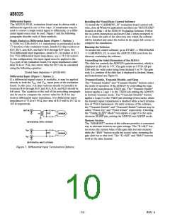
Output Bias, Impedance, and Termination
The differential output pins VOUT+ and VOUT– are also biased to a
dc level of approximately VCC/2. Therefore, the outputs should be
ac-coupled before being applied to the load. This is accomplished
with a 1:1 transformer as seen in the typical applications circuit
of Figure 6. The transformer also converts the output signal
from differential to single-ended, while maintaining a proper
impedance match to the line. The differential output impedance
of the AD8325 is internally maintained at 75 Ω, regardless of
whether the amplifier is in transmit enable mode (TXEN = 1)
or transmit disable mode (TXEN = 0). If the output signal is
being evaluated on standard 50 Ω test equipment, a 75 Ω to 50 Ω
pad must be used to provide the test circuit with the correct
impedance match.
Initial Power-Up
When the 5 V supply is first applied to the VCC pins of the
AD8325, the gain setting of the amplifier is indeterminate.
Therefore, as power is first applied to the amplifier, the TXEN
pin should be held low (Logic 0) thus preventing forward signal
transmission. After power has been applied to the amplifier, the
gain can be set to the desired level by following the procedure in
the SPI Programming and Gain Adjustment section. The TXEN
pin can then be brought from Logic 0 to 1, enabling forward
signal transmission at the desired gain level.
Power Supply Decoupling, Grounding, and Layout
Considerations
Between Burst Operation
Careful attention to printed circuit board layout details will
prevent problems due to associated board parasitics. Proper RF
design techniques are mandatory. The 5 V supply power should be
delivered to each of the VCC pins via a low impedance power bus
to ensure that each pin is at the same potential. The power bus
should be decoupled to ground with a 10 µF tantalum capacitor
located in close proximity to the AD8325. In addition to the
10 µF capacitor, each VCC pin should be individually decoupled to
ground with a 0.1 µF ceramic chip capacitor located as close to
the pin as possible. The pin labeled BYP (Pin 21) should also be
decoupled with a 0.1 µF capacitor. The PCB should have a low-
impedance ground plane covering all unused portions of the
component side of the board, except in the area of the input and
output traces (see Figure 10). It is important that all of the
AD8325’s ground pins are connected to the ground plane to
ensure proper grounding of all internal nodes. The differential
The asynchronous TXEN pin is used to place the AD8325 into
“Between Burst” mode while maintaining a differential output
impedance of 75 Ω. Applying a Logic 0 to the TXEN pin acti-
vates the on-chip reverse amplifier, providing a 74% reduction
in consumed power. The supply current is reduced from approxi-
mately 133 mA to approximately 35 mA. In this mode of
operation, between burst noise is minimized and the amplifier
can no longer transmit in the upstream direction. In addition to
the TXEN pin, the AD8325 also incorporates an asynchronous
SLEEP pin, which may be used to place the amplifier in a high
output impedance state and further reduce the supply current to
approximately 4 mA. Applying a Logic 0 to the SLEEP pin
places the amplifier into SLEEP mode. Transitioning into or
out of SLEEP mode will result in a transient voltage at the output
of the amplifier. Therefore, use only the TXEN pin for DOCSIS
compliant “Between Burst” operation.
5V
10F
25V
0.1F
AD8325 TSSOP
GND11
DATEN
V
IN–
0.1F
DATEN
SDATA
CLK
SDATA
CLK
V
CC6
Z
= 150⍀
IN
V
IN–
165⍀
0.1F
GND1
V
IN+
0.1F
0.1F
0.1F
V
GND10
CC
V
TXEN
TXEN
CC5
V
IN+
GND9
BYP
SLEEP
GND2
0.1F
0.1F
0.1F
V
V
V
1
CC
CC4
V
SLEEP
CC2
CC3
GND3
GND4
GND5
OUT–
GND8
GND7
GND6
OUT+
0.1F
TOKO 617DB-A0070
TO DIPLEXER Z = 75⍀
IN
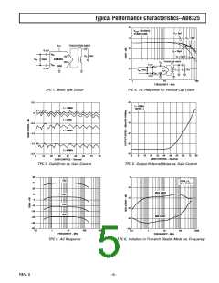
Figure 6. Typical Applications Circuit
–8–
REV. 0

 ADI [ ADI ]