AD8325
Distortion, Adjacent Channel Power, and DOCSIS
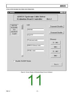
Evaluation Board Features and Operation
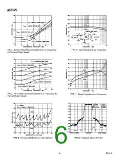
In order to deliver 58 dBmV of high fidelity output power required
by DOCSIS, the PA should be able to deliver about 61 dBmV
in order to make up for losses associated with the transformer
and diplexer. TPC 7 and TPC 8 show the AD8325 second and
third harmonic distortion performance versus fundamental
frequency for various output power levels. These figures are
useful for determining the inband harmonic levels from 5 MHz
to 65 MHz. Harmonics higher in frequency will be sharply attenu-
ated by the low-pass filter function of the diplexer. Another
measure of signal integrity is adjacent channel power or ACP.
DOCSIS section 4.2.9.1.1 states, “Spurious emissions from
a transmitted carrier may occur in an adjacent channel that could
be occupied by a carrier of the same or different symbol rates.”
TPC 12 shows the measured ACP for a 16 QAM, 61 dBmV signal,
taken at the output of the AD8325 evaluation board (see Figure
12 for evaluation board schematic). The transmit channel width
and adjacent channel width in TPC 12 correspond to symbol rates
of 160 KSYM/SEC. Table I shows the ACP results for the AD8325
for all conditions in DOCSIS Table 4-7 “Adjacent Channel
Spurious Emissions.”
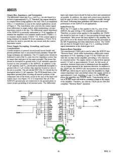
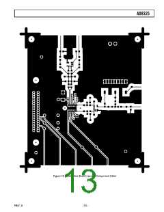
The AD8325 evaluation board (Part # AD8325-EVAL) and
control software can be used to control the AD8325 upstream
cable driver via the parallel port of a PC. A standard printer
cable connected between the parallel port and the evaluation
board is used to feed all the necessary data to the AD8325 by
means of the Windows-based, Microsoft Visual Basic control
software. This package provides a means of evaluating the
amplifier by providing a convenient way to program the gain/
attenuation as well as offering easy control of the amplifiers’
asynchronous TXEN and SLEEP pins. With this evaluation kit
the AD8325 can be evaluated with either a single-ended or differ-
ential input configuration. The amplifier can also be evaluated
with or without the PULSE diplexer in the output signal path. To
remove the diplexer from the signal path, leave R6 and R8 open
and install a 0 Ω chip resistor at R7. A schematic of the evalua-
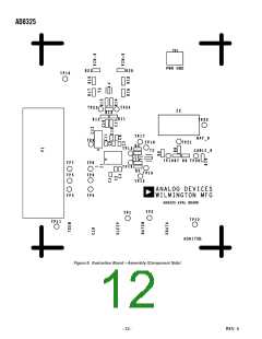
tion board is provided in Figure 12.
Table I. ACP Performance for All DOCSIS Conditions (All Values in dBc)
TRANSMIT
CHANNEL
SYMBOL
RATE
ADJACENT CHANNEL SYMBOL RATE
160 K
SYM/SEC
320 K
SYM/SEC
640 K
SYM/SEC
1280 K
SYM/SEC
2560 K
SYM/SEC
160 K
–53.8
–55.6
–61.1
–67.0
–66.7
SYM/SEC
320 K
640 K
–53.1
–54.3
–53.8
–53.2
–56.0
–54.0
–61.5
–56.3
–67.6
–62.0
SYM/SEC
SYM/SEC
1280 K
–56.3
–58.5
–54.3
–56.2
–53.4
–54.4
–54.1
–53.5
–56.3
–54.1
SYM/SEC
SYM/SEC
2560 K
Noise and DOCSIS
Overshoot on PC Printer Ports
At minimum gain, the AD8325’s output noise spectral density is
10 nV/√Hz measured at 10 MHz. DOCSIS Table 4-8, “Spurious
Emissions in 5 MHz to 42 MHz,” specifies the output noise for
various symbol rates. The calculated noise power in dBmV for
160 KSYM/SECOND is:
The data lines on some PC parallel printer ports have excessive
overshoot that may cause communications problems when pre-
sented to the CLK pin of the AD8325 (TP6 on the evaluation
board). The evaluation board was designed to accommodate a
series resistor and shunt capacitor (R2 and C5) to filter the
CLK signal if required.
2
Transformer and Diplexer
10 nV
20 log
×160 kHz + 60 = –48 dBmV
A 1:1 transformer is needed to couple the differential outputs of
the AD8325 to the cable while maintaining a proper impedance
match. The specified transformer is available from TOKO (Part
# 617DB-A0070); however, MA/COM part # ETC-1-1T-15
can also be used. The evaluation board is equipped with the
TOKO transformer, but is also designed to accept the MA/COM
transformer. The PULSE diplexer included on the evaluation
board provides a high-order low-pass filter function, typically
used in the upstream path. The ability of the PULSE diplexer
to achieve DOCSIS compliance is neither expressed nor implied
by Analog Devices Inc. Data on the diplexer can be obtained
from PULSE.
Hz
Comparing the computed noise power of –48 dBmV to the
8 dBmV signal yields –56 dBc, which meets the required level of
–53 dBc set forth in DOCSIS Table 4-8. As the AD8325’s gain is
increased from this minimum value, the output signal increases at a
faster rate than the noise, resulting in a signal to noise ratio that
improves with gain. In transmit disable mode, the output noise
spectral density computed over 160 KSYM/SECOND is 1.0 nV/√Hz
or –68 dBmV.
REV. 0
–9–

 ADI [ ADI ]