AD8132
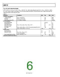
VOCM TO OUT SPECIFICATIONS
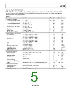
At TA = 25°C, VS = 5 V, VOCM = 2.5 V, G = 1, RL, dm = 499 Ω, RF = RG = 348 Ω, unless otherwise noted. For G = 2, RL, dm = 200 Ω, RF = 1000 Ω,
RG = 499 Ω. Refer to Figure 56 and Figure 57 for test setup and label descriptions. All specifications refer to single-ended input and
differential outputs, unless otherwise noted.
Table 4.
Parameter
Conditions
Min
Typ
Max
Unit
DYNAMIC PERFORMANCE
−3 dB Bandwidth
Slew Rate
Input Voltage Noise (RTI)
DC PERFORMANCE
Input Voltage Range
Input Resistance
Input Offset Voltage
Input Bias Current
VOCM CMRR
ΔVOCM = 600 mV p-p
ΔVOCM = 1.5 V to 3.5 V
f = 0.1 MHz to 100 MHz
210
340
12
MHz
V/μs
nV/√Hz
1.0 to 3.7
30
5
0.5
−66
1
V
kΩ
mV
μA
dB
VOS, cm = VOUT, cm; VDIN+ = VDIN− = VOCM = 2.5 V
11
ΔVOUT, dm/ΔVOCM; ΔVOCM = 2.5 V 1 V; resistors matched to 0.01%
ΔVOUT, cm/ΔVOCM; ΔVOCM = 2.5 V 1 V
Gain
0.985
1.015 V/V
POWER SUPPLY
Operating Range
Quiescent Current
2.7
9.4
11
12
V
VDIN+ = VDIN− = VOCM = 2.5 V
TMIN to TMAX variation
ΔVOUT, dm/ΔVS; ΔVS = 1 V
10.7
10
−70
mA
μA/°C
dB
Power Supply Rejection Ratio
−60
OPERATING TEMPERATURE RANGE
−40
+125 °C
Rev. F | Page 6 of 32

 ADI [ ADI ]