AD8132
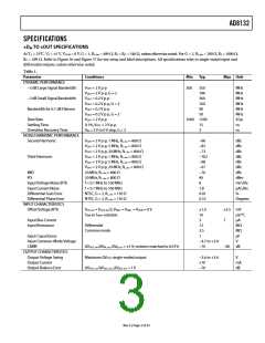
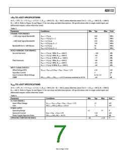
DIN TO OUT SPECIFICATIONS
At TA = 25°C, VS = 3 V, VOCM = 1.5 V, G = 1, RL, dm = 499 Ω, RF = RG = 348 Ω, unless otherwise noted. For G = 2, RL, dm = 200 Ω, RF = 1000 Ω,
RG = 499 Ω. Refer to Figure 56 and Figure 57 for test setup and label descriptions. All specifications refer to single-ended input and
differential outputs, unless otherwise noted.
Table 5.
Parameter
Conditions
Min Typ
Max Unit
DYNAMIC PERFORMANCE
−3 dB Large Signal Bandwidth
VOUT = 1 V p-p
VOUT = 1 V p-p, G = 2
VOUT = 0.2 V p-p
VOUT = 0.2 V p-p, G = 2
VOUT = 0.2 V p-p
VOUT = 0.2 V p-p, G = 2
350
165
350
150
45
MHz
MHz
MHz
MHz
MHz
MHz
−3 dB Small Signal Bandwidth
Bandwidth for 0.1 dB Flatness
50
NOISE/HARMONIC PERFORMANCE
Second Harmonic
VOUT = 1 V p-p, 1 MHz, RL, dm = 800 Ω
VOUT = 1 V p-p, 5 MHz, RL, dm = 800 Ω
VOUT = 1 V p-p, 20 MHz, RL, dm = 800 Ω
VOUT = 1 V p-p, 1 MHz, RL, dm = 800 Ω
VOUT = 1 V p-p, 5 MHz, RL, dm = 800 Ω
VOUT = 1 V p-p, 20 MHz, RL, dm = 800 Ω
−100
−94
−77
−90
−85
−66
dBc
dBc
dBc
dBc
dBc
dBc
Third Harmonic
INPUT CHARACTERISTICS
Offset Voltage (RTI)
Input Bias Current
Input Common-Mode Voltage
CMRR
VOS, dm = VOUT, dm/2; VDIN+ = VDIN− = VOCM = 1.5 V
10
3
0.3 to 1.0
−60
mV
μA
V
ΔVOUT, dm/ΔVIN, cm; ΔVIN, cm = 0.5 V; resistors matched to 0.01%
dB
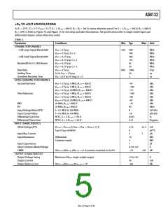
VOCM TO OUT SPECIFICATIONS
At TA = 25°C, VS = 3 V, VOCM = 1.5 V, G = 1, RL, dm = 499 Ω, RF = RG = 348 Ω, unless otherwise noted. For G = 2, RL, dm = 200 Ω, RF = 1000 Ω,
RG = 499 Ω. Refer to Figure 56 and Figure 57 for test setup and label descriptions. All specifications refer to single-ended input and
differential outputs, unless otherwise noted.
Table 6.
Parameter
Conditions
Min
Typ
Max
Unit
DC PERFORMANCE
Input Offset Voltage
Gain
VOS, cm = VOUT, cm; VDIN+ = VDIN− = VOCM = 1.5 V
ΔVOUT, cm/ΔVOCM; ΔVOCM = 0.5 V
7
1
mV
V/V
POWER SUPPLY
Operating Range
Quiescent Current
Power Supply Rejection Ratio
OPERATING TEMPERATURE RANGE
2.7
11
V
VDIN+ = VDIN− = VOCM = 0 V
ΔVOUT, dm/ΔVS; ΔVS = 0.5 V
7.25
−70
mA
dB
°C
−40
+125
Rev. F | Page 7 of 32

 ADI [ ADI ]