AD8132
ABSOLUTE MAXIMUM RATINGS
Table 7.
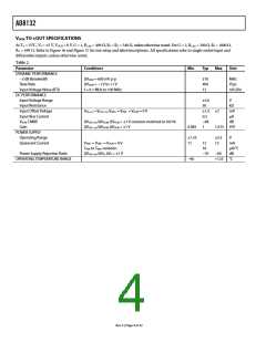
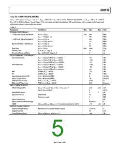
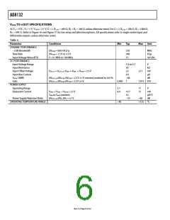
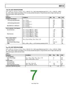
The power dissipated in the package (PD) is the sum of the
quiescent power dissipation and the power dissipated in the
package due to the load drive for all outputs. The quiescent
power is the voltage between the supply pins (VS) times the
quiescent current (IS). The load current consists of the dif-
ferential and common-mode currents flowing to the load, as
well as currents flowing through the external feedback net-
works and the internal common-mode feedback loop. The
internal resistor tap used in the common-mode feedback loop
places a 1 kΩ differential load on the output. Consider rms
voltages and currents when dealing with ac signals.
Parameter
Rating
Supply Voltage
5.5 V
VOCM
VS
Internal Power Dissipation
Operating Temperature Range
Storage Temperature Range
Lead Temperature (Soldering 10 sec)
Junction Temperature
250 mW
−40°C to +125°C
−65°C to +150°C
300°C
150°C
Stresses above those listed under Absolute Maximum Ratings
may cause permanent damage to the device. This is a stress
rating only; functional operation of the device at these or any
other conditions above those indicated in the operational
section of this specification is not implied. Exposure to absolute
maximum rating conditions for extended periods may affect
device reliability.
Airflow reduces θJA. In addition, more metal directly in contact
with the package leads from metal traces through holes, ground,
and power planes reduces the θJA.
Figure 3 shows the maximum safe power dissipation in the
package vs. the ambient temperature for the 8-lead SOIC_N
(θJA = 121°C/W) and MSOP (θJA = 142°C/W) packages on a
JEDEC standard 4-layer board. θJA values are approximations.
THERMAL RESISTANCE
θJA is specified for the worst-case conditions, that is, θJA is
specified for the device soldered in a circuit board in still air.
1.75
Table 8.
Package Type
1.50
1.25
θJA
Unit
°C/W
°C/W
8-Lead SOIC/4-Layer
8-Lead MSOP/4-Layer
121
142
1.00
Maximum Power Dissipation
SOIC
The maximum safe power dissipation in the AD8132 packages
is limited by the associated rise in junction temperature (TJ) on
the die. At approximately 150°C (the glass transition temperature),
the plastic changes its properties. Even temporarily exceeding
this temperature limit can change the stresses that the package
exerts on the die, permanently shifting the parametric performance
of the AD8132. Exceeding a junction temperature of 150°C for
an extended period can result in changes in the silicon devices,
potentially causing failure.
0.75
MSOP
0.50
0.25
0
–40 –30 –20 –10
0
10 20 30 40 50 60 70 80 90 100 110 120
AMBIENT TEMPERATURE (°C)
Figure 3. Maximum Power Dissipation vs. Temperature
ESD CAUTION
Rev. F | Page 8 of 32

 ADI [ ADI ]