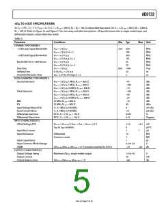
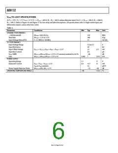
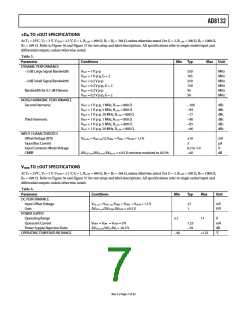
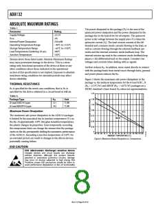
AD8132
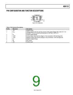
PIN CONFIGURATION AND FUNCTION DESCRIPTIONS
AD8132
–IN
1
2
3
4
8
7
6
5
+IN
NC
V
OCM
V+
V–
+OUT
–OUT
NC = NO CONNECT
Figure 4. Pin Configuration
Table 9. Pin Function Descriptions
Pin No.
Mnemonic
Description
Negative Input.
1
2
−IN
VOCM
Voltage applied to this pin sets the common-mode output voltage with a ratio of 1:1. For
example, 1 V dc on VOCM sets the dc bias level on +OUT and −OUT to 1 V.
3
4
5
6
7
8
V+
Positive Supply Voltage.
Positive Output. Note that the voltage at −DIN is inverted at +OUT (see Figure 64).
Negative Output. Note that the voltage at +DIN is inverted at −OUT (see Figure 64).
Negative Supply Voltage.
No Connect.
+OUT
−OUT
V−
NC
+IN
Positive Input.
Rev. F | Page 9 of 32

 ADI [ ADI ]