AD8132
TABLE OF CONTENTS
Features .............................................................................................. 1
Differential Amplifier Without Resistors (High Input
Impedance Inverting Amplifier).............................................. 21
Applications....................................................................................... 1
General Description......................................................................... 1
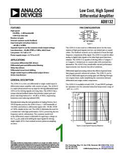
Pin Configuration............................................................................. 1
Revision History ............................................................................... 2
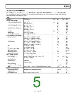
Specifications..................................................................................... 3
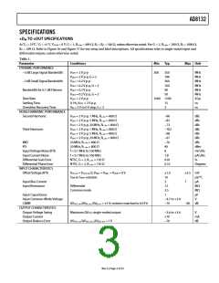
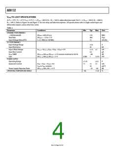
DIN to OUT Specifications...................................................... 3
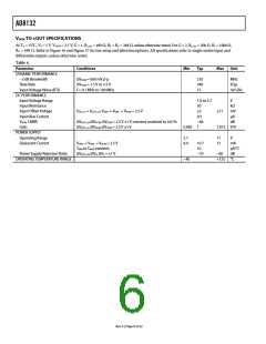
VOCM to OUT Specifications ..................................................... 4
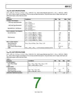
DIN to OUT Specifications...................................................... 5
VOCM to OUT Specifications ..................................................... 6
DIN to OUT Specifications...................................................... 7
VOCM to OUT Specifications ..................................................... 7
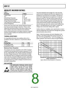
Absolute Maximum Ratings............................................................ 8
Thermal Resistance ...................................................................... 8
ESD Caution.................................................................................. 8
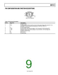
Pin Configuration and Function Descriptions............................. 9
Typical Performance Characteristics ........................................... 10
Test Circuits..................................................................................... 19
Operational Description................................................................ 20
Definition of Terms.................................................................... 20
Basic Circuit Operation............................................................. 20
Theory of Operation ...................................................................... 21
General Usage of the AD8132 .................................................. 21
Other β2 = 1 Circuits................................................................. 22
Varying β2 ................................................................................... 22
β1 = 0............................................................................................ 22
Estimating the Output Noise Voltage...................................... 22
Calculating Input Impedance of the Application Circuit ..... 23
Input Common-Mode Voltage Range in Single-Supply
Applications ................................................................................ 23
Setting the Output Common-Mode Voltage.......................... 23
Driving a Capacitive Load......................................................... 23
Open-Loop Gain and Phase ..................................................... 23
Layout, Grounding, and Bypassing.............................................. 24
Circuits......................................................................................... 24
Applications..................................................................................... 25
Analog-to-Digital Driver .......................................................... 25
Balanced Cable Driver............................................................... 25
Transmit Equalizer..................................................................... 26
Low-Pass Differential Filter ...................................................... 26
High Common-Mode Output Impedance Amplifier ........... 27
Full-Wave Rectifier .................................................................... 28
Outline Dimensions....................................................................... 29
Ordering Guide .......................................................................... 29
REVISION HISTORY
11/06—Rev. E to Rev. F
12/04—Rev. C to Rev. D
Updated Format..................................................................Universal
Changes to Table 1............................................................................ 3
Changes to Table 4............................................................................ 6
Changes to Table 5............................................................................ 7
Changes to Ordering Guide .......................................................... 29
Changes to General Description .....................................................1
Changes to Specifications.................................................................2
Changes to Absolute Maximum Ratings........................................8
Updated Outline Dimensions....................................................... 29
Changes to Ordering Guide.......................................................... 29
11/05—Rev. D to Rev. E
2/03—Rev. B to Rev. C
Changes to Table 7, Thermal Resistance Section, Maximum
Power Dissipation Section, and Figure 3....................................... 8
Changes to Ordering Guide .......................................................... 29
Changes to Specifications.................................................................2
Addition to Estimating the Output Noise Voltage Section....... 15
Updated Outline Dimensions....................................................... 21
1/02—Rev. A to Rev. B
Edits to Transmitter Equalizer Section........................................ 18
Rev. F | Page 2 of 32

 ADI [ ADI ]