Data Sheet
AD7904/AD7914/AD7924
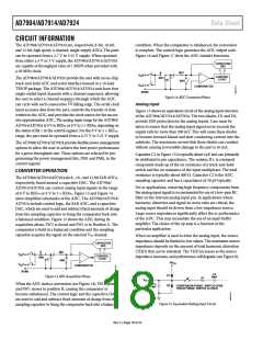
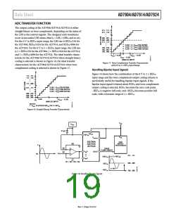
ADC TRANSFER FUNCTION
The output coding of the AD7904/AD7914/AD7924 is either
straight binary or twos complement, depending on the status of
the LSB in the control register. The designed code transitions
occur at successive LSB values (that is, 1 LSB, 2 LSBs, and so on).
For the 0 V to REFIN input range, the LSB size is REFIN/256 for
the AD7904, REFIN/1024 for the AD7914, and REFIN/4096 for
the AD7924. For the 0 V to 2 × REFIN input range, the LSB size
is 2 × REFIN/256 for the AD7904, 2 × REFIN/1024 for the AD7914,
and 2 × REFIN/4096 for the AD7924. The ideal transfer charac-
teristic for the AD7904/AD7914/AD7924 when straight binary
coding is selected is shown in Figure 16; the ideal transfer
characteristic for the AD7904/AD7914/AD7924 when twos
complement coding is selected is shown in Figure 17.
011…111
011…110
•
•
000…001
000…000
111…111
•
•
1LSB = 2 × V
1LSB = 2 × V
1LSB = 2 × V
/256 AD7904
/1024 AD7914
/4096 AD7924
REF
REF
REF
100…010
100…001
100…000
–V
+ 1LSB
+V – 1LSB
REF
REF
V
– 1LSB
REF
ANALOG INPUT
Figure 17. Twos Complement Transfer Characteristic
with 0 V to 2 × REFIN Input Range
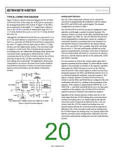
Handling Bipolar Input Signals
Figure 18 shows how the combination of the 0 V to 2 × REFIN
input range and the twos complement output coding scheme is
particularly useful for handling bipolar input signals. If the
bipolar input signal is biased about REFIN and twos complement
output coding is selected, REFIN becomes the zero code point,
−REFIN is negative full scale, and +REFIN becomes positive full
scale, with a dynamic range of 2 × REFIN.
111…111
111…110
•
•
111…000
•
1LSB = V
1LSB = V
1LSB = V
/256 AD7904
/1024 AD7914
/4096 AD7924
011…111
REF
REF
REF
•
•
000…010
000…001
000…000
1LSB
+V
– 1LSB
REF
0V
ANALOG INPUT
NOTES
1. V
IS EITHER REF OR 2 × REF
.
REF
IN IN
Figure 16. Straight Binary Transfer Characteristic
V
DD
V
REF
0.1µF
AV
DD
REF
IN
V
DD
V
DRIVE
AD7904/
AD7914/
AD7924
DSP/
R4
R1
MICRO-
V
PROCESSOR
R3
TWOS
COMPLEMENT
V
V
0
DOUT
IN
R2
V
0V
011…111
000…000
100…000
(= 2 × REF
)
+REF
IN
IN
3
IN
R1 = R2 = R3 = R4
REF
IN
IN
(= 0V)
–REF
Figure 18. Handling Bipolar Signals
Rev. C | Page 19 of 32

 ADI [ ADI ]