Data Sheet
AD7904/AD7914/AD7924
CONTROL REGISTER
The control register of the AD7904/AD7914/AD7924 is a
12-bit, write-only register. Data is loaded from the DIN pin of
the AD7904/AD7914/AD7924 on the falling edge of SCLK. The
data is transferred on the DIN line at the same time that the
conversion result is read from the part. The data transferred on
the DIN line corresponds to the AD7904/AD7914/AD7924
configuration for the next conversion. This requires 16 serial
clocks for every data transfer. Only the information provided
loaded to the control register. MSB denotes the first bit in the
data stream. The bit functions are outlined in Table 8.
Table 7. Channel Selection
ADD1
ADD0
Analog Input Channel
0
0
1
1
0
1
0
1
VIN0
VIN1
VIN2
VIN3
CS
on the first 12 falling clock edges (after the
falling edge) is
Table 8. Control Register Bit Functions
MSB
LSB
11
10
9
8
7
6
5
4
3
2
1
0
WRITE
SEQ1
DONTC
DONTC
ADD1
ADD0
PM1
PM0
SEQ0
DONTC
RANGE
CODING
Bit
Mnemonic Description
11
WRITE
The value written to this bit determines whether the following 11 bits will be loaded to the control register. If this bit
is set to 1, the following 11 bits will be written to the control register; if this bit is set to 0, the remaining 11 bits are not
loaded to the control register, which remains unchanged.
10
SEQ1
The SEQ1 bit is used in conjunction with the SEQ0 bit to control the use of the sequencer function (see Table 10).
Don’t care bits.
[9:8] DONTC
[7:6] ADD1,
ADD0
The two address bits are loaded at the end of the present conversion sequence and select which analog input
channel is to be converted in the next serial transfer, or they may select the final channel in a consecutive sequence
as described in Table 10. The selected input channel is decoded as shown in Table 7. The address bits corresponding
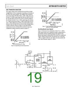
to the conversion result are also output on DOUT prior to the 12 bits of data (see the Serial Interface section). The next
channel to be converted on will be selected by the mux on the 14th SCLK falling edge.
[5:4] PM1, PM0
The two power management bits decode the mode of operation of the AD7904/AD7914/AD7924 as described in
Table 9.
3
2
1
SEQ0
DONTC
RANGE
The SEQ0 bit is used in conjunction with the SEQ1 bit to control the use of the sequencer function (see Table 10).
Don’t care bit.
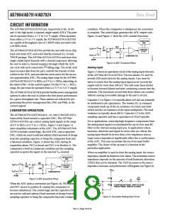
This bit selects the analog input range to be used on the AD7904/AD7914/AD7924. If it is set to 0, the analog input
range will extend from 0 V to 2 × REFIN. If it is set to 1, the analog input range will extend from 0 V to REFIN (for the next
conversion). For the 0 V to 2 × REFIN input range, VDD = 4.75 V to 5.25 V.
0
CODING
This bit selects the type of output coding that the AD7904/AD7914/AD7924 will use for the conversion result. If this
bit is set to 0, the output coding for the part will be twos complement. If this bit is set to 1, the output coding from
the part will be straight binary (for the next conversion).
Table 9. Power Mode Selection
PM1
PM0
Mode
Description
1
1
Normal
operation
In normal operation mode, the AD7904/AD7914/AD7924 remain in full power mode regardless of
the status of any of the logic inputs. This mode allows the fastest possible throughput rate from the
AD7904/AD7914/AD7924.
1
0
0
1
Full
shutdown
In full shutdown mode, the AD7904/AD7914/AD7924 are in full shutdown with all circuitry on the
device powering down. The AD7904/AD7914/AD7924 retain the information in the control register
while in full shutdown. The part remains in full shutdown until these bits are changed.
In auto shutdown mode, the AD7904/AD7914/AD7924 automatically enter full shutdown mode at the
end of each conversion when the control register is updated. Wake-up time from full shutdown is 1 μs;
the user should ensure that 1 μs has elapsed before attempting to perform a valid conversion on the
part in this mode.
Auto
shutdown
0
0
Invalid
Invalid selection. This configuration is not allowed.
Rev. C | Page 15 of 32

 ADI [ ADI ]