AD7904/AD7914/AD7924
Data Sheet
MODES OF OPERATION
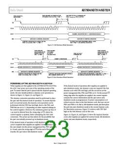
The AD7904/AD7914/AD7924 have three modes of operation.
These modes are designed to provide flexible power management
options. These options can be chosen to optimize the power
dissipation/throughput rate ratio for differing application require-
ments. The mode of operation of the AD7904/AD7914/AD7924
is controlled by the power management bits, PM1 and PM0, in
the control register (see Table 9). When power supplies are first
applied to the AD7904/AD7914/AD7924, care should be taken to
ensure that the part is placed in the required mode of operation
(see the Powering Up the AD7904/AD7914/AD7924 section).
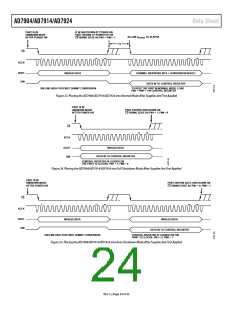
FULL SHUTDOWN MODE (PM1 = 1, PM0 = 0)
In full shutdown mode, all internal circuitry on the AD7904/
AD7914/AD7924 is powered down. The part retains information
in the control register during full shutdown. The AD7904/AD7914/
AD7924 remain in full shutdown until the power management
bits in the control register, PM1 and PM0, are changed.
If a write to the control register occurs while the part is in full
shutdown, and the power management bits are changed to
PM0 = PM1 = 1 (that is, normal mode), the part will begin to
CS
power up on the
rising edge. The track-and-hold, which was
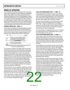
NORMAL MODE (PM1 = PM0 = 1)
in hold mode while the part was in full shutdown, returns to
track mode on the 14th SCLK falling edge.
Normal mode is intended for the fastest throughput rate perfor-
mance. Because the AD7904/AD7914/AD7924 remain fully
powered up at all times, the user does not need to worry about
power-up times. Figure 20 shows the general diagram of the
operation of the AD7904/AD7914/AD7924 in this mode.
To ensure that the part is fully powered up, tPOWER-UP (t12) should
CS
have elapsed before the next
falling edge. Figure 21 shows
the general diagram for this sequence.
AUTO SHUTDOWN MODE (PM1 = 0, PM0 = 1)
CS
In auto shutdown mode, the AD7904/AD7914/AD7924 auto-
matically enter shutdown at the end of each conversion when
the control register is updated. When the part is in auto shutdown,
the track-and-hold is in hold mode. Figure 22 shows the general
diagram of the operation of the AD7904/AD7914/AD7924 in
this mode.
1
16
12
SCLK
DOUT
2 LEADING ZEROS + 2 CHANNEL IDENTIFIER BITS
+ CONVERSION RESULT
DATA IN TO CONTROL REGISTER
DIN
NOTES
1. CONTROL REGISTER DATA IS LOADED ON FIRST 12 SCLK CYCLES.
In auto shutdown mode, all internal circuitry on the AD7904/
AD7914/AD7924 is powered down. The part retains information
in the control register during auto shutdown. The AD7904/
Figure 20. Normal Mode Operation
CS
The conversion is initiated on the falling edge of ; the track-
CS
AD7914/AD7924 remain in shutdown until the next
falling
falling edge, the track-and-hold,
and-hold enters hold mode as described in the Serial Interface
section. The data presented to the AD7904/AD7914/AD7924
on the DIN line during the first 12 clock cycles of the data
transfer is loaded into the control register (provided that the
WRITE bit is set to 1). In normal mode, the part remains fully
powered up at the end of the conversion as long as the PM1 and
PM0 bits are set to 1 in the write transfer during that same
conversion. To ensure continued operation in normal mode,
PM1 and PM0 must both be set to 1 on every data transfer,
assuming that a write operation is taking place. If the WRITE
bit is set to 0, the power management bits are left unchanged,
and the part remains in normal mode.
CS
edge that it receives. On this
which was in hold mode while the part was in shutdown, returns
to track mode. Wake-up time from auto shutdown is 1 µs max-
imum, and the user should ensure that 1 µs has elapsed before
attempting a valid conversion.
When running the AD7904/AD7914/AD7924 with a 20 MHz
clock, one 16 SCLK dummy cycle should be sufficient to ensure
that the part is fully powered up. During this dummy cycle, the
contents of the control register should remain unchanged;
therefore, the WRITE bit should be set to 0 on the DIN line.
This dummy cycle effectively halves the throughput rate of the
part, with every other conversion result being valid. In auto
shutdown mode, the power consumption of the part is greatly
reduced because the part enters shutdown at the end of each
conversion. When the control register is programmed to move
into auto shutdown mode, it does so at the end of the con-
version. The user can move the ADC in and out of the low
Sixteen serial clock cycles are required to complete the conversion
and to access the conversion result. The track-and-hold returns
CS
to track mode on the 14th SCLK falling edge.
high until the next conversion or it may idle low until some
CS
may then idle
time prior to the next conversion (effectively idling
low).
When a data transfer is complete (DOUT has returned to three-
state), another conversion can be initiated after the quiet time,
CS
power state by controlling the
signal.
CS
tQUIET, has elapsed by bringing
low again.
Rev. C | Page 22 of 32

 ADI [ ADI ]