AD7904/AD7914/AD7924
Data Sheet
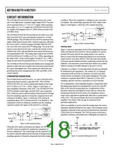
Analog Input Selection
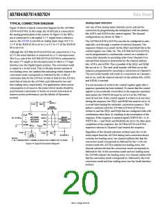
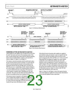
TYPICAL CONNECTION DIAGRAM
Any one of four analog input channels can be selected for
conversion by programming the multiplexer with the address
bits ADD1 and ADD0 in the control register. The channel
configurations are shown in Table 7.
Figure 19 shows a typical connection diagram for the AD7904/
AD7914/AD7924. In this setup, the AGND pin is connected to
the analog ground plane of the system. In Figure 19, the REFIN
pin is connected to a decoupled 2.5 V supply from a reference
source, the AD780, to provide an analog input range of 0 V to
2.5 V (if the RANGE bit is set to 1) or 0 V to 5 V (if the RANGE
bit is set to 0).
The AD7904/AD7914/AD7924 can also be configured to auto-
matically cycle through a number of selected channels. The
sequencer feature is accessed via the SEQ1 and SEQ0 bits in the
control register (see Table 10). The AD7904/AD7914/AD7924
can be programmed to continuously convert on a number of
consecutive channels in ascending order from Channel 0 to a
selected final channel as determined by the channel address
bits, ADD1 and ADD0. This is possible if the SEQ1 and SEQ0
bits are set to 11. The next serial transfer will then act on the
sequence programmed by executing a conversion on Channel 0.
The next serial transfer will result in a conversion on Channel 1,
and so on, until the channel selected via the address bits, ADD1
and ADD0, is reached.
Although the AD7904/AD7914/AD7924 are connected to a VDD
of 5 V, the serial interface is connected to a 3 V microprocessor.
The VDRIVE pin of the AD7904/AD7914/AD7924 is connected to
the same 3 V supply as the microprocessor to allow a 3 V logic
interface (see the Digital Inputs section). The conversion result
is output in a 16-bit word. This 16-bit data stream consists of
two leading zeros, two address bits indicating which channel the
conversion result corresponds to, followed by the 12 bits of
conversion data for the AD7924 (10 bits of data for the AD7914
and 8 bits of data for the AD7904, each followed by two and
four trailing zeros, respectively). For applications where power
consumption is of concern, the power-down modes should be
used between conversions or bursts of several conversions to
improve power performance (see the Modes of Operation
section).
It is not necessary to write to the control register again after a
sequence operation has been initiated. To ensure that the control
register is not accidently overwritten or the sequence operation
interrupted, the WRITE bit must be set to 0 or the DIN line
must be tied low. If the control register is written to at any time
during the sequence, the SEQ1 and SEQ0 bits must be set to 10
to avoid interrupting the automatic conversion sequence. This
pattern continues until the AD7904/AD7914/AD7924 are
written to and the SEQ1 and SEQ0 bits are configured with a bit
combination other than 10, resulting in the termination of the
sequence. If the sequence is uninterrupted (WRITE bit = 0, or
WRITE bit = 1 and SEQ1 and SEQ0 bits are set to 10), then upon
completion of the sequence, the AD7904/AD7914/AD7924
sequencer returns to Channel 0 and restarts the sequence.
5V
SUPPLY
0.1µF
10µF
SERIAL
INTERFACE
AV
DD
V
V
0
3
SCLK
IN
MICRO-
CONTROLLER/
MICRO-
AD7904/
AD7914/
AD7924
0V TO REF
IN
DOUT
CS
IN
PROCESSOR
DIN
AGND
REF
V
DRIVE
IN
Regardless of the channel selection method used, the 16-bit
word output from the AD7924 during each conversion always
contains two leading zeros, two channel address bits that the
conversion result corresponds to, followed by the 12-bit con-
version result; the AD7914 outputs two leading zeros, two
channel address bits that the conversion result corresponds to,
followed by the 10-bit conversion result and two trailing zeros;
the AD7904 outputs two leading zeros, two channel address bits
that the conversion result corresponds to, followed by the 8-bit
conversion result and four trailing zeros (see the Serial Interface
section).
0.1µF
0.1µF
10µF
2.5V
AD780
3V SUPPLY
NOTES
1. ALL UNUSED INPUT CHANNELS SHOULD BE CONNECTED TO AGND.
Figure 19. Typical Connection Diagram
Rev. C | Page 20 of 32

 ADI [ ADI ]