AD7873
Data Sheet
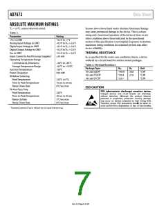
ABSOLUTE MAXIMUM RATINGS
TA = 25°C, unless otherwise noted.
Stresses above those listed under Absolute Maximum Ratings
may cause permanent damage to the device. This is a stress
rating only; functional operation of the device at these or any
other conditions above those indicated in the operational
section of this specification is not implied. Exposure to absolute
maximum rating conditions for extended periods may affect
device reliability.
Table 3.
Parameter
Rating
+VCC to GND
–0.3 V to +7 V
Analog Input Voltage to GND
Digital Input Voltage to GND
Digital Output Voltage to GND
VREF to GND
Input Current to Any Pin Except Supplies1
Operating Temperature Range
Commercial (A, B Versions)
Storage Temperature Range
Junction Temperature
Power Dissipation
–0.3 V to VCC + 0.3 V
–0.3 V to VCC + 0.3 V
–0.3 V to VCC + 0.3 V
–0.3 V to VCC + 0.3 V
±10 mA
THERMAL RESISTANCE
θJA is specified for the worst-case conditions, that is, a device
soldered in a circuit board for surface-mount packages.
–ꢀ0°C to +85°C
–±5°C to +150°C
150°C
Table 4. Thermal Resistance
Package Type
1±-Lead QSOP
1±-Lead TSSOP
1±-Lead LFCSP
θJA
θJC
Unit
°C/W
°C/W
°C/W
1ꢀ9.97
150.ꢀ
135.7
38.8
27.±
ꢀ50 mW
IR Reflow Soldering
Peak Temperature
Time-to-Peak Temperature
Ramp-Down Rate
220°C (±5°C)
10 sec to 30 sec
±°C/sec max
ESD CAUTION
Pb-free Parts Only
Peak Temperature
250°C
Time-to-Peak Temperature
Ramp-Up Rate
Ramp-Down Rate
20 sec to ꢀ0 sec
3°C/sec max
±°C/sec max
1 Transient currents of up to 100 mA do not cause SCR latch-up.
Rev. F | Page ± of 28

 ADI [ ADI ]