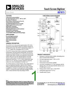
AD7873
Data Sheet
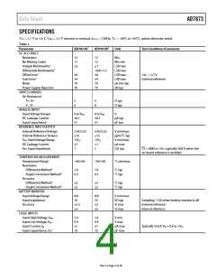
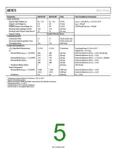
Parameter
AD7873A1
AD7873B1
Unit
Test Conditions/Comments
LOGIC OUTPUTS
Output High Voltage, VOH
Output Low Voltage, VOL
PENIRQ Output Low Voltage, VOL
Floating-State Leakage Current
Floating-State Output Capacitance5
Output Coding
VCC – 0.2
0.ꢀ
0.ꢀ
VCC – 0.2
0.ꢀ
0.ꢀ
V min
ISOURCE = 250 µA; VCC = 2.2 V to 5.25 V
ISINK = 250 µA
100 kΩ pull-up; ISINK = 250 µA
V max
V max
µA max
pF max
±10
10
±10
10
Straight (Natural) Binary
CONVERSION RATE
Conversion Time
Track-and-Hold Acquisition Time
Throughput Rate
12
3
125
12
3
125
DCLK cycles max
DCLK cycles min
kSPS max
POWER REQUIREMENTS
+VCC (Specified Performance)
ICC
2.7/3.±
2.7/3.±
V min/max
Functional from 2.2 V to 5.25 V
Digital I/Ps = 0 V or VCC
±
Normal Mode (fSAMPLE = 125 kSPS)
380
±70
380
±70
170
150
580
1
µA max
µA typ
µA typ
µA typ
µA typ
µA max
Internal reference off, VCC = 3.± V, 2ꢀ0 µA typ
Internal reference on, VCC = 3.± V
Internal reference off, VCC = 2.7 V, fDCLK = 200 kHz
Internal reference off, VCC = 3.± V
Internal reference on, VCC = 3.± V
200 nA typ
Normal Mode (fSAMPLE = 12.5 kSPS) 170
Normal Mode (Static)
150
580
1
Shutdown Mode (Static)
Power Dissipation±
Normal Mode (fSAMPLE = 125 kSPS)
1.3±8
2.ꢀ12
3.±
1.3±8
2.ꢀ12
3.±
mW max
mW typ
µW max
Internal reference off, VCC = 3.± V
Internal reference on, VCC = 3.± V
VCC = 3.± V
Shutdown
1 Temperature range as follows: A, B Versions: –ꢀ0°C to +85°C.
2 See the Terminology section.
3 Difference between TEMP0 and TEMP1 measurement. No calibration necessary.
ꢀ Temperature drift is –2.1 mV/°C.
5 Sample tested @ 25°C to ensure compliance.
± See the Power vs. Throughput Rate section.
Rev. F | Page ꢀ of 28

 ADI [ ADI ]