Data Sheet
AD7873
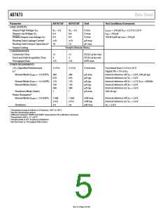
TIMING SPECIFICATIONS
TA = TMIN to TMAX, unless otherwise noted; VCC = 2.7 V to 5.25 V, VREF = 2.5 V.
Table 2. Timing Specifications1
Parameter
Limit at TMIN, TMAX
Unit
Description
2
fDCLK
10
2
1.5
10
kHz min
MHz max
µs min
ns min
ns max
ns max
ns min
ns min
ns max
ns min
ns min
ns max
ns min
ns max
ns max
tACQ
t1
Acquisition time
CS falling edge to first DCLK rising edge
CS falling edge to busy three-state disabled
CS falling edge to DOUT three-state disabled
DCLK high pulse width
t2
±0
3
t3
±0
tꢀ
t5
t±
t7
t8
200
200
±0
10
10
DCLK low pulse width
DCLK falling edge to BUSY rising edge
Data setup time prior to DCLK rising edge
Data valid to DCLK hold time
Data access time after DCLK falling edge
CS rising edge to DCLK ignored
3
t9
200
0
t10
t11
CS rising edge to BUSY high impedance
CS rising edge to DOUT high impedance
100
100
ꢀ
t12
1 Sample tested at 25°C to ensure compliance. All input signals are specified with tr = tf = 5 ns (10% to 90% of VCC) and timed from a voltage level of 1.± V.
2 Mark/space ratio for the DCLK input is ꢀ0/±0 to ±0/ꢀ0.
3 Measured with the load circuit of Figure 2 and defined as the time required for the output to cross 0.ꢀ V or 2.0 V.
ꢀ t12 is derived from the measured time taken by the data outputs to change 0.5 V when loaded with the circuit of Figure 2. The measured number is then extrapolated
back to remove the effects of charging or discharging the 50 pF capacitor. This means that the time, t12, quoted in the timing characteristics is the true bus relinquish
time of the part and is independent of the bus loading.
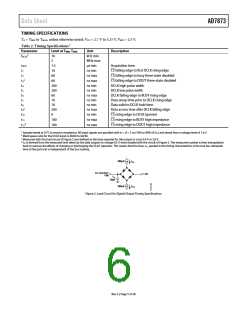
200µA
I
OL
TO OUTPUT
PIN
1.6V
C
L
50pF
200µA
I
OH
Figure 2. Load Circuit for Digital Output Timing Specifications
Rev. F | Page 5 of 28

 ADI [ ADI ]