AD7873
Data Sheet
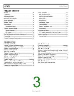
TABLE OF CONTENTS
Features .............................................................................................. 1
Circuit Information........................................................................ 13
ADC Transfer Function............................................................. 13
Typical Connection Diagram ................................................... 13
Analog Input ............................................................................... 14
Measurements............................................................................. 16
Pen Interrupt Request................................................................ 18
Control Register ......................................................................... 19
Power vs. Throughput Rate....................................................... 20
Serial Interface............................................................................ 21
Grounding and Layout .................................................................. 23
PCB Design Guidelines for Chip Scale Package .................... 23
Outline Dimensions....................................................................... 24
Ordering Guide .......................................................................... 25
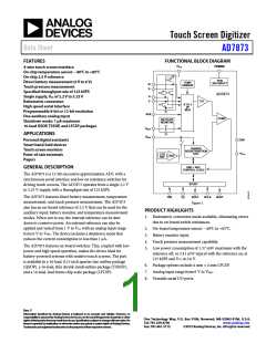
Applications....................................................................................... 1
General Description......................................................................... 1
Functional Block Diagram .............................................................. 1
Product Highlights ........................................................................... 1
Revision History ............................................................................... 2
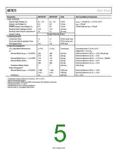
Specifications..................................................................................... 3
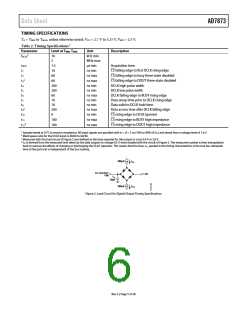
Timing Specifications .................................................................. 5
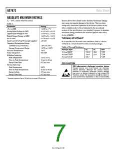
Absolute Maximum Ratings............................................................ 6
Thermal Resistance ...................................................................... 6
ESD Caution.................................................................................. 6
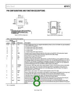
Pin Configurations and Function Descriptions ........................... 7
Terminology ...................................................................................... 8
Typical Performance Characteristics ............................................. 9
REVISION HISTORY
2/13—Rev. E to Rev. F
4/03—Rev. B to Rev. C
Changes to General Description Section ...................................... 1
Added EPAD Note to Figure 3 and Table 5................................... 7
Updated Outline Dimensions....................................................... 24
Changes to Ordering Guide .......................................................... 26
Changes to Formatting ......................................................Universal
Updated Outline Dimensions....................................................... 19
1/02—Rev. A to Rev. B
Addition of 16-Lead Lead Frame Chip Scale Package ..Universal
Edits to Features.................................................................................1
Edits to General Description ...........................................................1
Addition of LFCSP Pin Configuration ...........................................4
Edit to Absolute Maximum Ratings................................................4
Addition to Ordering Guide ............................................................4
Addition of CP-16 Outline Dimensions .................................... 19
9/06—Rev. D to Rev. E
Changes to Figure 13 Caption ...................................................... 10
Updated Outline Dimensions....................................................... 24
Changes to Ordering Guide .......................................................... 25
6/04—Rev. C to Rev. D
Updated Format..................................................................Universal
Changes to Absolute Maximum Ratings....................................... 6
Additions to PD0 and PD1 Description...................................... 21
PBC Guidelines for Chip Scale Package Added ......................... 23
Additions to Ordering Guide........................................................ 25
2/01—Rev. 0 to Rev A
Edits to Notes in the Ordering Guide
Rev. F | Page 2 of 28

 ADI [ ADI ]