AD7870/AD7875/AD7876
MICRO P RO CESSO R INTERFACE
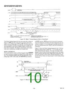
T he AD7870/AD7875/AD7876 has a wide variety of interfacing
options. It offers two operating modes and three data-output for-
mats. Fast data access times allow direct interfacing to most mi-
croprocessors including the DSP processors.
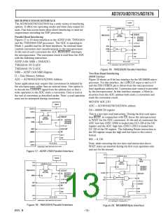
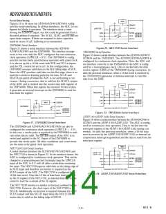
P ar allel Read Inter facing
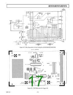
Figures 17 to 19 show interfaces to the ADSP-2100, T MS32010
and the T MS32020 DSP processors. T he ADC is operating in
Mode 1, parallel read for all three interfaces. An external timer
controls conversion start asynchronously to the microprocessor.
At the end of each conversion the ADC BUSY/INT interrupts
the microprocessor. T he conversion result is read from the ADC
with the following instruction:
2
ADSP-2100: MR0 = DM(ADC)
T MS32010: IN D,ADC
T MS32020: IN D,ADC
Figure 19. TMS32020 Parallel Interface
MR0 = ADSP-2100 MR0 Register
D = Data Memory Address
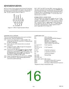
Two Byte Read Inter facing
68008 Interface
ADC = AD7870/AD7875/AD7876 Address
Figure 20 shows an 8-bit bus interface for the MC68008 micro-
processor. For this interface, the 12/8/CLK input is tied to 0 V
and the DB11/HBEN pin is driven from the microprocessor
least significant address bit. Conversion start control is provided
by the microprocessor. In this interface example, a Move in-
struction from the ADC address both starts a conversion and
reads the conversion result.
Some applications may require that conversions be initiated by
the microprocessor rather than an external timer. One option is
to decode the CONVST signal from the address bus so that a
write operation to the ADC starts a conversion. Data is read at
the end of conversion as described earlier. Note: a read operation
must not be attempted during conversion.
MOVEW ADC,DO
ADC = AD7870/AD7875/AD7876 address
D0 = 68008 D0 register
T his is a two byte read instruction. During the first read opera-
tion BUSY, in conjunction with CS, forces the microprocessor
to WAIT for the ADC conversion. At the end of conversion the
ADC low byte (DB7–DB0) is loaded into D15–D8 of the D0
register and the ADC high byte (DB15–DB7) is loaded into
D7–D0 of the D0 register. T he following Rotate instruction to
the D0 register swaps the high and low bytes to the correct
format.
R0L = 8, D0.
Note: while executing the two byte read instruction above,
WAIT states are inserted during the first read operation only
and not for the second.
Figure 17. ADSP-2100 Parallel Interface
Figure 18. TMS32010 Parallel Interface
Figure 20. MC68008 Byte Interface
REV. B
–13–

 ADI [ ADI ]