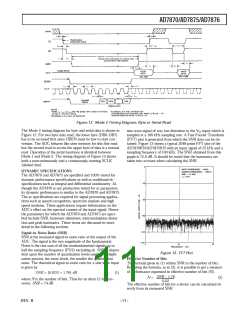
AD7870/AD7875/AD7876
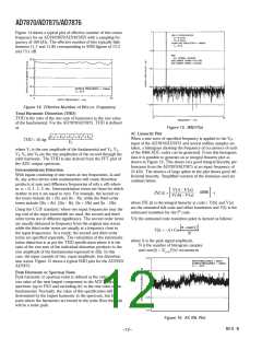
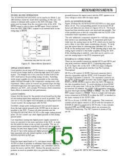
STAND -ALO NE O P ERATIO N
grounds between the signal source and the ADC appears as an
error voltage in series with the input signal.
T he AD7870/AD7875/AD7876 can be used in its Mode 2, par-
allel interface mode for stand-alone operation. In this case, con-
version is initiated with a pulse to the ADC CS input. T his
pulse must be longer than the conversion time of the ADC. T he
BUSY output is used to drive the RD input. Data is latched
from the ADC DB0–DB11 outputs to an external latch on the
rising edge of BUSY.
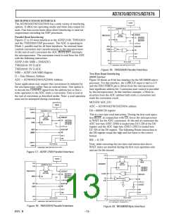
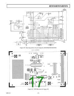
D ATA ACQ UISITIO N BO ARD
Figure 28 shows the AD7870/AD7875/AD7876 in a data acqui-
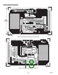
sition circuit. T he corresponding printed circuit board (PCB)
layout and silkscreen are shown in Figures 29 to 31. T he board
layout has three interface ports: one serial and two parallel. One
of the parallel ports is directly compatible with the ADSP-2100
evaluation board expansion connector.
T he only additional component required for a full data acquisi-
tion system is an antialiasing filter. A component grid is pro-
vided near the analog input on the PCB, which may be used for
such a filter or any other input conditioning circuitry. T o facili-
tate this option there is a shorting plug (labelled LK1 on the
PCB) on the analog input track. If this shorting plug is used, the
analog input connects to the buffer amplifier driving the ADC;
if this shorting plug is omitted, a wire link can be used to con-
nect the analog input to the PCB component grid.
2
INTERFACE CO NNECTIO NS
T here are two parallel connectors labeled SKT 4 and SKT 6 and
one serial connector labeled SKT 5. A shorting plug option
(LK3 in Figure 28) on the ADC 12/8/CLK input configures
the ADC for the appropriate interface (see Pin Function
Description).
Figure 25. Stand-Alone Operation
AP P LICATIO N H INTS
Good printed circuit board (PCB) layout is as important as the
overall circuit design itself in achieving high speed A/D perfor-
mance. T he designer has to be conscious of noise both in the
ADC itself and in the preceding analog circuitry. Switching
mode power supplies are not recommended as the switching
spikes will feed through to the comparator causing noisy code
transitions. Other causes of concern are ground loops and digi-
tal feedthrough from microprocessors. T hese are factors which
influence any ADC, and a proper PCB layout which minimizes
these effects is essential for best performance.
SKT 6 is a 96-contact (3-ROW) Eurocard connector that is
directly compatible with the ADSP-2100 Evaluation Board
Prototype Expansion Connector. T he expansion connector on
the ADSP-2100 has eight decoded chip enable outputs labeled
ECE1 to ECE8. ECE6 is used to drive the ADC CS input on
the data acquisition board. T o avoid selecting on board RAM
sockets at the same time, LK6 on the ADSP-2100 board must
be removed. In addition, the ADSP-2100 expansion connector
has four interrupts labelled EIRQ0 to EIRQ3. T he ADC BUSY/
INT output connects to EIRQ0. T here is a single wait state gen-
erator connected to EDMACK to allow the ADC to interface to
the faster versions of the ADSP-2100.
LAYO UT H INTS
Ensure that the layout for the printed circuit board has the digi-
tal and analog signal lines separated as much as possible. T ake
care not to run any digital track alongside an analog signal track.
Guard (screen) the analog input with AGND.
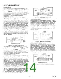
SKT 4 is a 26-way (2-ROW) IDC connector. T his connector
contains all the signal contacts as SKT 6 with the exception of
EDMACK which is connected to SKT 6 only. It also contains
decoded R/W and STRB inputs which are necessary for
T MS32020 interfacing. T he SKT 4 pinout is shown in Fig-
ure 26.
Establish a single point analog ground (star ground) separate
from the logic system ground at the AGND pin or as close as
possible to the ADC. Connect all other grounds and the
AD7870/AD7875/AD7876 DGND to this single analog ground
point. Do not connect any other digital grounds to this analog
ground point.
Low impedance analog and digital power supply common re-
turns are essential to low noise operation of the ADC, so make
the foil width for these tracks as wide as possible. T he use of
ground planes minimizes impedance paths and also guards the
analog circuitry from digital noise. T he circuit layout of Figures
30 and 31 have both analog and digital ground planes which are
kept separated and only joined together at the AD7870/
AD7875/AD7876 AGND pin.
NO ISE
Keep the input signal leads to VIN and signal return leads from
AGND as short as possible to minimize input noise coupling. In
applications where this is not possible, use a shielded cable be-
tween the source and the ADC. Reduce the ground circuit im-
pedance as much as possible since any potential difference in
Figure 26. SKT4, IDC Connector Pinout
REV. B
–15–

 ADI [ ADI ]