AD7870/AD7875/AD7876
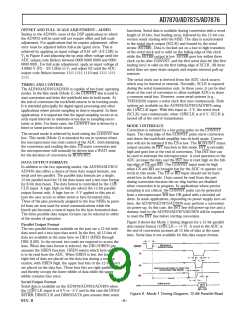
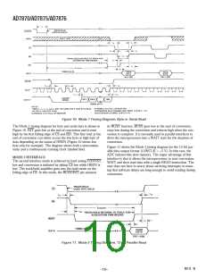
Figure 10. Mode 1 Tim ing Diagram , Byte or Serial Read
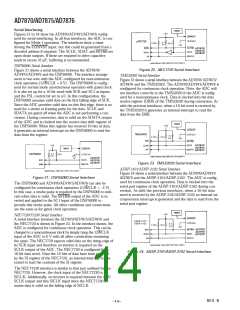
T he Mode 1 timing diagram for byte and serial data is shown in
Figure 10. INT goes low at the end of conversion and is reset
high by the first falling edge of CS and RD. T his first read at the
end of conversion can either access the low byte or high byte of
data depending on the status of HBEN (Figure 10 shows low
byte only for example). T he diagram shows both a noncontinu-
ously and a continuously running clock (dashed line).
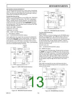
its BUSY function. BUSY goes low at the start of conversion,
stays low during the conversion and returns high when the con-
version is complete. It is normally used in parallel interfaces to
drive the microprocessor into a WAIT state for the duration of
conversion.
Figure 11 shows the Mode 2 timing diagram for the 12-bit par-
allel data output format (12/8/CLK = +5 V). In this case, the
ADC behaves like slow memory. T he major advantage of this
interface is that it allows the microprocessor to start conversion,
WAIT and then read data with a single READ instruction. T he
user does not have to worry about servicing interrupts or ensur-
ing that software delays are long enough to avoid reading during
conversion.
MO D E 2 INTERFACE
T he second interface mode is achieved by hard wiring CONVST
low and conversion is initiated by taking CS low while HBEN is
low. T he track/hold amplifier goes into the hold mode on the
falling edge of CS. In this mode, the BUSY/INT pin assumes
Figure 11. Mode 2 Tim ing Diagram , 12-Bit Parallel Read
REV. B
–10–

 ADI [ ADI ]