AD7870/AD7875/AD7876
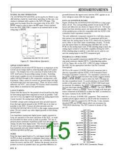
SKT 5 is a 9-way D-type connector that is meant for serial inter-
facing only. An inverted DB9/SCLK output is also provided on
this connector for systems that accept data on a rising clock
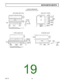
edge. T he SKT 5 pinout is shown in Figure 27.
SKT 1, SKT 2 and SKT 3 are three BNC connectors which pro-
vide input connections for the analog input, the CONVST input
and an external clock input. T he use of an external clock source
is optional; there is a shorting plug (LK2) on the ADC CLK in-
put that must be connected to either –5 V (for the ADCs own
internal clock) or to SKT 3.
P O WER SUP P LY CO NNECTIO NS
T he PCB requires two analog power supplies and one 5 V digi-
tal supply . T he analog supplies are labelled V+ and V–, and the
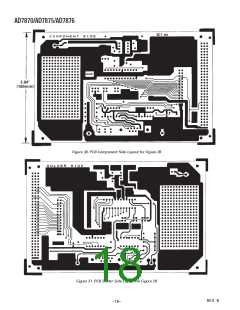
range for both supplies is 12 V to 15 V (see silkscreen in Figure
29). Connection to the 5 V digital supply is made through any
of the connectors (SKT 4 to SKT 6). T he –5 V supply required
by the ADC is generated from a voltage regulator on the V–
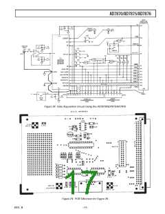
power supply input (IC3 in Figure 27).
Figure 27. SKT5, D-Type Connector Pinout
SH O RTING P LUG O P TIO NS
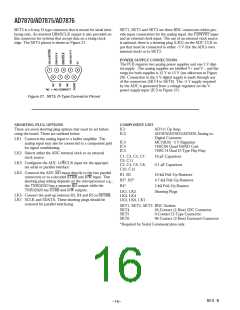
CO MP O NENT LIST
T here are seven shorting plug options that must be set before
using the board. T hese are outlined below:
IC1
IC2
AD711 Op Amp
AD7870/AD7875/AD7876 Analog-to-
Digital Converter
MC79L05 –5 V Regulator
74HC00 Quad NAND Gate
74HC74 Dual D-T ype Flip Flop
LK1 Connects the analog input to a buffer amplifier. T he
analog input may also be connected to a component grid
for signal conditioning.
IC3
IC4
IC5
LK2 Selects either the ADC internal clock or an external
clock source.
C1, C3, C5, C7,
C9, C11
C2, C4, C6, C8,
C10, C12
10 µF Capacitors
LK3 Configures the ADC 12/8/CLK input for the appropri-
0.1 µF Capacitors
ate serial or parallel interface.
LK4 Connects the ADC RD input directly to the two parallel
connectors or to a decoded STRB and R/W input. T his
shorting plug setting depends on the microprocessor e.g.,
the T MS32010 has a separate RD output while the
T MS32020 has STRB and R/W outputs.
R1, R2
R3*, R5*
R4*
10 kΩ Pull-Up Resistors
4.7 kΩ Pull-Up Resistors
2 kΩ Pull-Up Resistor
Shorting Plugs
LK1, LK2
LK5– Connect the pull-up resistors R3, R4 and R5 to SSTRB,
LK7 SCLK and SDAT A. T hese shorting plugs should be
removed for parallel interfacing.
LK3, LK4
LK5, LK6, LK7
SKT 1, SKT 2, SKT 3 BNC Sockets
SKT 4
SKT 5
SKT 6
26-Contact (2-Row) IDC Connector
9-Contact D-T ype Connector
96-Contact (3-Row) Eurocard Connector
*Required for Serial Communication only.
REV. B
–16–

 ADI [ ADI ]