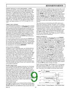
AD7870/AD7875/AD7876
O FFSET AND FULL-SCALE AD JUSTMENT—AD 7875
Similar to the AD7870, most of the DSP applications in which
the AD7875 will be used will not require offset and full-scale
adjustment. For applications that do require adjustment, offset
error must be adjusted before full-scale (gain) error. T his is
achieved by applying an input voltage of 0.61 mV (1/2 LSB) to
V1 in Figure 8 and adjusting the op amp offset voltage until the
ADC output code flickers between 0000 0000 0000 and 0000
0000 0001. For full-scale adjustment, apply an input voltage of
4.9982 V (FS – 3/2 LSBs) to V1 and adjust R2 until the ADC
output code flickers between 1111 1111 1110 and 1111 1111
1111.
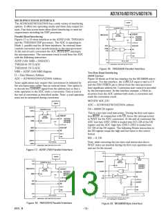
functions. Serial data is available during conversion with a word
length of 16 bits; four leading zeros, followed by the 12-bit con-
version result starting with the MSB. T he data is synchronized
to the serial clock output (SCLK) and framed by the serial
strobe (SSTRB). Data is clocked out on a low to high transition
of the serial clock and is valid on the falling edge of this clock
while the SSTRB output is low. SSTRB goes low within three
clock cycles after CONVST, and the first serial data bit (the first
leading zero) is valid on the first falling edge of SCLK. All three
serial lines are open-drain outputs and require external pull-up
resistors.
2
The serial clock out is derived from the ADC clock source,
which may be internal or external. Normally, SCLK is required
during the serial transmission only. In these cases, it can be shut
down at the end of conversion to allow multiple ADCs to share
a common serial bus. However, some serial systems (e.g.,
T MS32020) require a serial clock that runs continuously. Both
options are available on the AD7870/AD7875/AD7876 using
the 12/8/CLK input. With this input at –5 V, the serial clock
(SCLK) runs continuously; when 12/8/CLK is at 0 V, SCLK is
turned off at the end of transmission.
TIMING AND CO NTRO L
The AD7870/AD7875/AD7876 is capable of two basic operating
modes. In the first mode (Mode 1), the CONVST line is used to
start conversion and drive the track/hold into its hold mode. At
the end of conversion the track/hold returns to its tracking mode.
It is intended principally for digital signal processing and other
applications where precise sampling in time is required. In these
applications, it is important that the signal sampling occurs at ex-
actly equal intervals to minimize errors due to sampling uncer-
tainty or jitter. For these cases, the CONVST line is driven by a
timer or some precise clock source.
MO D E 1 INTERFACE
Conversion is initiated by a low going pulse on the CONVST
input. T he rising edge of this CONVST pulse starts conversion
and drives the track/hold amplifier into its hold mode. Conver-
sion will not be initiated if the CS is low. T he BUSY/INT status
output assumes its INT function in this mode. INT is normally
high and goes low at the end of conversion. T his INT line can
be used to interrupt the microprocessor. A read operation to the
ADC accesses the data and the INT line is reset high on the fall-
ing edge of CS and RD. T he CONVST input must be high
when CS and RD are brought low for the ADC to operate cor-
rectly in this mode. T he CS or RD input should not be hard-
wired low in this mode. Data cannot be read from the part
during conversion because the on-chip latches are disabled
when conversion is in progress. In applications where precise
sampling is not critical, the CONVST pulse can be generated
from a microprocessor WR line OR-gated with a decoded ad-
dress. In some applications, depending on power supply turn-on
time, the AD7870/AD7875/AD7876 may perform a conversion
on power-up. In this case, the INT line will power-up low and a
dummy read to the AD7870/AD7875/AD7876 will be required
to reset the INT line before starting conversion.
T he second mode is achieved by hard-wiring the CONVST line
low. T his mode (Mode 2) is intended for use in systems where
the microprocessor has total control of the ADC, both initiating
the conversion and reading the data. CS starts conversion and
the microprocessor will normally be driven into a WAIT state
for the duration of conversion by BUSY/INT.
D ATA O UTP UT FO RMATS
In addition to the two operating modes, the AD7870/AD7875/
AD7876 also offers a choice of three data output formats, one
serial and two parallel. T he parallel data formats are a single,
12-bit parallel word for 16-bit data buses and a two-byte format
for 8-bit data buses. T he data format is controlled by the 12/8/
CLK input. A logic high on this pin selects the 12-bit parallel
output format only. A logic low or –5 V applied to this pin al-
lows the user access to either serial or byte formatted data.
T hree of the pins previously assigned to the four MSBs in paral-
lel form are now used for serial communications while the
fourth pin becomes a control input for the byte-formatted data.
T he three possible data output formats can be selected in either
of the modes of operation.
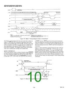
Figure 9 shows the Mode 1 timing diagram for a 12-bit parallel
data output format (12/8/CLK = +5 V). A read to the ADC at
the end of conversion accesses all 12 bits of data at the same
time. Serial data is not available for this data output format.
P ar allel O utput For m at
T he two parallel formats available on the part are a 12-bit wide
data word and a two-byte data word. In the first, all 12 bits of
data are available at the same time on DB11 (MSB) through
DB0 (LSB). In the second, two reads are required to access the
data. When this data format is selected, the DB11/HBEN pin
assumes the HBEN function. HBEN selects which byte of data
is to be read from the ADC. When HBEN is low, the lower
eight bits of data are placed on the data bus during a read op-
eration; with HBEN high, the upper four bits of the 12-bit word
are placed on the data bus. T hese four bits are right justified
and thereby occupy the lower nibble of data while the upper
nibble contains four zeros.
Ser ial O utput For m at
Serial data is available on the AD7870/AD7875/AD7876 when
the 12/8/CLK input is at 0 V or –5 V and in this case the DB10/
SSTRB, DB9/SCLK and DB8/SDAT A pins assume their serial
Figure 9. Mode 1 Tim ing Diagram , 12-Bit Parallel Read
REV. B
–9–

 ADI [ ADI ]