AD7715
The on-chip oscillator circuit also has a start-up time associated
with it before it is oscillating at its correct frequency and correct
voltage levels. The typical start-up time for the circuit is 10 ms
with a DVDD of +5 V and 15 ms with a DVDD of +3 V. At 3 V
supplies, depending on the loading capacitances on the MCLK
pins, a 1 MΩ feedback resistor may be required across the crys-
tal or resonator in order to keep the start up times around the
15 ms duration.
conditions after a RESET and it is generally necessary to set up
all registers and carry out a calibration after a RESET command.
The AD7715’s on-chip oscillator circuit continues to function
even when the RESET input is low. The master clock signal
continues to be available on the MCLK OUT pin. Therefore, in
applications where the system clock is provided by the AD7715’s
clock, the AD7715 produces an uninterrupted master clock
during RESET commands.
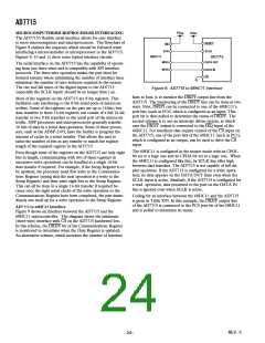
The AD7715’s master clock appears on the MCLK OUT pin of
the device. The maximum recommended load on this pin is one
CMOS load. When using a crystal or ceramic resonator to gen-
erate the AD7715’s clock, it may be desirable to then use this
clock as the clock source for the system. In this case, it is recom-
mended that the MCLK OUT signal is buffered with a CMOS
buffer before being applied to the rest of the circuit.
Standby Mode
The STBY bit in the Communications Register of the AD7715
allows the user to place the part in a power-down mode when it
is not required to provide conversion results. The AD7715
retains the contents of all its on-chip registers (including the
data register) while in standby mode. When released from
standby mode, the part starts to process data and a new word is
available in the data register in 3 × 1/Output Rate from when a 0
is written to the STBY bit.
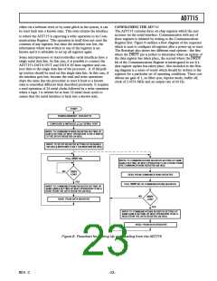
System Synchronization
The FSYNC bit of the Setup Register allows the user to reset
the modulator and digital filter without affecting any of the
setup conditions on the part. This allows the user to start gath-
ering samples of the analog input from a known point in time,
i.e., when the FSYNC is changed from 1 to 0.
The STBY bit does not affect the digital interface, and it does
not affect the status of the DRDY line. If DRDY is high when
the STBY bit is brought low, it will remain high until there is a
valid new word in the data register. If DRDY is low when the
STBY bit is brought low, it will remain low until the data regis-
ter is updated at which time the DRDY line will return high for
500 × tCLK IN before returning low again. If DRDY is low when
the part enters its standby mode (indicating a valid unread word
in the data register), the data register can be read while the part
is in standby. At the end of this read operation, the DRDY will
be reset high as normal.
With a 1 in the FSYNC bit of the Setup Register, the digital
filter and analog modulator are held in a known reset state and
the part is not processing any input samples. When a 0 is then
written to the FSYNC bit, the modulator and filter are taken
out of this reset state and on the next master clock edge the part
starts to gather samples again.
The FSYNC input can also be used as a software start convert
command allowing the AD7715 to be operated in a conven-
tional converter fashion. In this mode, writing to the FSYNC bit
starts conversion and the falling edge of DRDY indicates when
conversion is complete. The disadvantage of this scheme is that
the settling time of the filter has to be taken into account for
every data register update. This means that the rate at which the
data register is updated is three times slower in this mode.
Placing the part in standby mode reduces the total current to
5 µA typical when the part is operated from an external master
clock provided this master clock is stopped. If the external clock
continues to run in standby mode, the standby current increases
to 150 µA typical with 5 V supplies and 75 µA typical with 3.3 V
supplies. If a crystal or ceramic resonator is used as the clock
source, then the total current in standby mode is 400 µA typical
with 5 V supplies and 90 µA with 3.3 V supplies. This is because
the on-chip oscillator circuit continues to run when the part is in
its standby mode. This is important in applications where the
system clock is provided by the AD7715’s clock, so that the
AD7715 produces an uninterrupted master clock even when it is
in its standby mode.
Since the FSYNC bit resets the digital filter, the full settling
time of 3 × 1/Output Rate must elapse before there is a new
word loaded to the output register on the part. If the DRDY
signal is low when FSYNC goes to a 0, the DRDY signal will
not be reset high by the FSYNC command. This is because the
AD7715 recognizes that there is a word in the data register that
has not been read. The DRDY line will stay low until an update
of the data register takes place at which time it will go high for
500 × tCLK IN before returning low again. A read from the data
register resets the DRDY signal high, and it will not return low
until the settling time of the filter has elapsed (from the FSYNC
command) and there is a valid new word in the data register. If
the DRDY line is high when the FSYNC command is issued,
the DRDY line will not return low until the settling time of the
filter has elapsed.
Accuracy
Sigma-delta ADCs, like VFCs and other integrating ADCs, do
not contain any source of nonmonotonicity and inherently offer
no missing codes performance. The AD7715 achieves excellent
linearity by the use of high quality, on-chip capacitors, which
have a very low capacitance/voltage coefficient. The device also
achieves low input drift through the use of chopper-stabilized
techniques in its input stage. To ensure excellent performance
over time and temperature, the AD7715 uses digital calibration
techniques which minimize offset and gain error.
Reset Input
The RESET input on the AD7715 resets all the logic, the digital
filter and the analog modulator while all on-chip registers are
reset to their default state. DRDY is driven high and the AD7715
ignores all communications to any of its registers while the
RESET input is low. When the RESET input returns high, the
AD7715 starts to process data, and DRDY will return low in
3 × 1/Output Rate indicating a valid new word in the data
register. However, the AD7715 operates with its default setup
Drift Considerations
The AD7715 uses chopper stabilization techniques to minimize
input offset drift. Charge injection in the analog switches and
dc leakage currents at the sampling node are the primary
sources of offset voltage drift in the converter. The dc input
leakage current is essentially independent of the selected gain.
Gain drift within the converter depends primarily upon the
temperature tracking of the internal capacitors. It is not af-
fected by leakage currents.
REV. C
–20–

 ADI [ ADI ]