AD7715
package allows the user to evaluate the true performance of the
part, independent of the analog input signal. The scheme
involves using a test mode on the part where the differential
inputs to the AD7715 are internally shorted together to provide
a zero differential voltage for the analog modulator. External to
the device, the AIN(–) input should be connected to a voltage
which is within the allowable common-mode range of the part.
This scheme should be used after a calibration has been per-
formed on the part.
is complete. It also goes high prior to the updating of the output
register to indicate when not to read from the device to ensure
that a data read is not attempted while the register is being
updated. CS is used to select the device. It can be used to de-
code the AD7715 in systems where a number of parts are con-
nected to the serial bus.
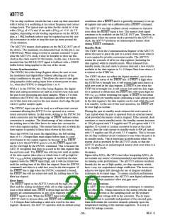
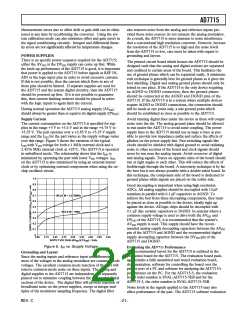
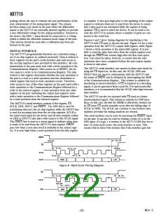
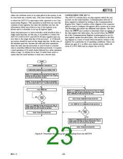
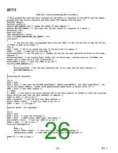
Figures 6 and 7 show timing diagrams for interfacing to the
AD7715 with CS used to decode the part. Figure 6 is for a read
operation from the AD7715’s output shift register, while Figure
7 shows a write operation to the input shift register. It is pos-
sible to read the same data twice from the output register even
though the DRDY line returns high after the first read opera-
tion. Care must be taken, however, to ensure that the read
operations have been completed before the next output update
is about to take place.
DIGITAL INTERFACE
The AD7715’s programmable functions are controlled using a
set of on-chip registers as outlined previously. Data is written to
these registers via the part’s serial interface and read access to
the on-chip registers is also provided by this interface. All com-
munications to the part must start with a write operation to the
Communications Register. After power-on or RESET, the de-
vice expects a write to its Communications Register. The data
written to this register determines whether the next operation to
the part is a read or a write operation and also determines to
which register this read or write operation occurs. Therefore,
write access to any of the other registers on the part starts with a
write operation to the Communications Register followed by a
write to the selected register. A read operation from any other
register on the part (including the output data register) starts
with a write operation to the Communications Register followed
by a read operation from the selected register.
The AD7715 serial interface can operate in three-wire mode by
tying the CS input low. In this case, the SCLK, DIN and
DOUT lines are used to communicate with the AD7715 and
the status of DRDY can be obtained by interrogating the MSB
of the Communications Register. This scheme is suitable for
interfacing to microcontrollers. If CS is required as a decoding
signal, it can be generated from a port bit. For microcontroller
interfaces, it is recommended that the SCLK idles high between
data transfers.
The AD7715 can also be operated with CS used as a frame
synchronization signal. This scheme is suitable for DSP inter-
faces. In this case, the first bit (MSB) is effectively clocked out
by CS since CS would normally occur after the falling edge of
SCLK in DSPs. The SCLK can continue to run between data
transfers provided the timing numbers are obeyed.
The AD7715’s serial interface consists of five signals, CS,
SCLK, DIN, DOUT and DRDY. The DIN line is used for
transferring data into the on-chip registers while the DOUT line
is used for accessing data from the on-chip registers. SCLK is
the serial clock input for the device and all data transfers (either
on DIN or DOUT) take place with respect to this SCLK signal.
The DRDY line is used as a status signal to indicate when data
is ready to be read from the AD7715’s data register. DRDY
goes low when a new data word is available in the output regis-
ter. It is reset high when a read operation from the data register
The serial interface can be reset by exercising the RESET input
on the part. It can also be reset by writing a series of 1s on the
DIN input. If a logic 1 is written to the AD7715 DIN line for at
least 32 serial clock cycles, the serial interface is reset. This
ensures that in three-wire systems that if the interface gets lost
DRDY
t10
t3
CS
t4
t8
t6
SCLK
t7
t5
t9
DOUT
MSB
LSB
Figure 6. Read Cycle Timing Diagram
CS
t16
t11
t14
SCLK
t15
t12
t13
LSB
DIN
MSB
Figure 7. Write Cycle Timing Diagram
REV. C
–22–

 ADI [ ADI ]