AD7715
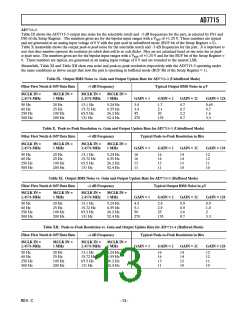
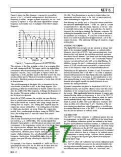
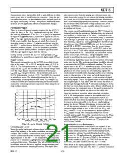
Figure 4 shows the filter frequency response for a cutoff fre-
quency of 15.72 Hz which corresponds to a first filter notch
frequency of 60 Hz. The plot is shown from dc to 390 Hz. This
response is repeated at either side of the digital filter’s sample
frequency and at either side of multiples of the filter’s sample
frequency.
26.2 Hz. Post-filtering can be applied to this to reduce the
bandwidth and output noise, to the 7.86 Hz bandwidth level,
while maintaining an output rate of 100 Hz.
Post-filtering can also be used to reduce the output noise from
the device for bandwidths below 13.1 Hz. At a gain of 128 and
a bandwidth of 13.1 Hz, the output rms noise is 520 nV. This
is essentially device noise or white noise and since the input is
chopped, the noise has a primarily flat frequency response. By
reducing the bandwidth below 13.1 Hz, the noise in the result-
ant passband can be reduced. A reduction in bandwidth by a
factor of 2 results in a reduction of approximately 1.25 in the
output rms noise. This additional filtering will result in a longer
settling time.
0
–20
–40
–60
–80
–100
–120
–140
–160
–180
–200
–220
–240
ANALOG FILTERING
The digital filter does not provide any rejection at integer mul-
tiples of the modulator sample frequency, as outlined earlier.
However, due to the AD7715’s high oversampling ratio, these
bands occupy only a small fraction of the spectrum and most
broadband noise is filtered. This means that the analog filtering
requirements in front of the AD7715 are considerably reduced
versus a conventional converter with no on-chip filtering. In
addition, because the part’s common-mode rejection perfor-
mance of 95 dB extends out to several kHz, common-mode
noise in this frequency range will be substantially reduced.
0
60
180
FREQUENCY – Hz
120
300
360
240
Figure 4. Frequency Response of AD7715 Filter
The response of the filter is similar to that of an averaging filter
but with a sharper roll-off. The output rate for the digital filter
corresponds with the positioning of the first notch of the filter’s
frequency response. Thus, for the plot of Figure 4 where the
output rate is 60 Hz, the first notch of the filter is at 60 Hz. The
notches of this (sinx/x)3 filter are repeated at multiples of the
first notch. The filter provides attenuation of better than 100 dB
at these notches.
Depending on the application, however, it may be necessary to
provide attenuation prior to the AD7715 in order to eliminate
unwanted frequencies from these bands which the digital filter
will pass. It may also be necessary in some applications to pro-
vide analog filtering in front of the AD7715 to ensure that dif-
ferential noise signals outside the band of interest do not
saturate the analog modulator.
The cutoff frequency of the digital filter is determined by the
value loaded to bits FS0 to FS1 in the Setup Register. Pro-
gramming a different cutoff frequency via FS0 and FS1 does not
alter the profile of the filter response; it changes the frequency of
the notches. The output update of the part and the frequency of
the first notch correspond.
If passive components are placed in front of the AD7715, in
unbuffered mode, care must be taken to ensure that the source
impedance is low enough so as not to introduce gain errors in
the system. This significantly limits the amount of passive anti-
aliasing filtering which can be provided in front of the AD7715
when it is used in unbuffered mode. However, when the part is
used in buffered mode, large source impedances will simply
result in a small dc offset error (a 10 kΩ source resistance will
cause an offset error of less than 10 µV). Therefore, if the sys-
tem requires any significant source impedances to provide pas-
sive analog filtering in front of the AD7715, it is recommended
that the part be operated in buffered mode.
Since the AD7715 contains this on-chip, low-pass filtering,
there is a settling time associated with step function inputs and
data on the output will be invalid after a step change until the
settling time has elapsed. The settling time depends upon the
output rate chosen for the filter. The settling time of the filter
to a full-scale step input can be up 4 times the output data
period. For a synchronized step input (using the FSYNC func-
tion), the settling time is 3 times the output data period.
CALIBRATION
Post-Filtering
The AD7715 provides a number of calibration options that can
be programmed via the MD1 and MD0 bits of the Setup Regis-
ter. The different calibration options are outlined in the Setup
Register and Calibration Sequences sections. A calibration cycle
may be initiated at any time by writing to these bits of the Setup
Register. Calibration on the AD7715 removes offset and gain
errors from the device. A calibration routine should be initiated
on the device whenever there is a change in the ambient operat-
ing temperature or supply voltage. It should also be initiated if
there is a change in the selected gain, filter notch or bipolar/
unipolar input range.
The on-chip modulator provides samples at a 19.2 kHz output
rate with fCLK IN at 2.4576 MHz. The on-chip digital filter
decimates these samples to provide data at an output rate which
corresponds to the programmed output rate of the filter. Since
the output data rate is higher than the Nyquist criterion, the
output rate for a given bandwidth will satisfy most application
requirements. However, there may be some applications which
require a higher data rate for a given bandwidth and noise per-
formance. Applications that need this higher data rate will
require some post-filtering following the digital filter of the
AD7715.
The AD7715 offers self-calibration and system-calibration facili-
ties. For full calibration to occur on the selected channel, the
on-chip microcontroller must record the modulator output for
two different input conditions. These are “zero-scale” and
For example, if the required bandwidth is 7.86 Hz but the re-
quired update rate is 100 Hz, the data can be taken from the
AD7715 at the 100 Hz rate giving a –3 dB bandwidth of
REV. C
–17–

 ADI [ ADI ]