AD7715
either via a software error or by some glitch in the system, it can
be reset back into a known state. This state returns the interface
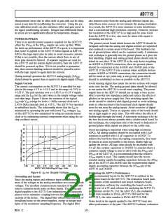
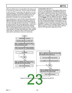
CONFIGURING THE AD7715
The AD7715 contains three on-chip registers which the user
accesses via the serial interface. Communication with any of
these registers is initiated by writing to the Communications
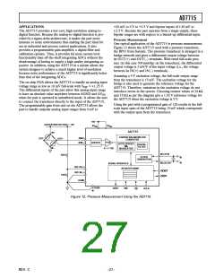
Register first. Figure 8 outlines a flow diagram of the sequence
which is used to configure all registers after a power-up or reset.
The flowchart also shows two different read options—the first
where the DRDY pin is polled to determine when an update of
the data register has taken place, the second where the DRDY
bit of the Communications Register is interrogated to see if a
data register update has taken place. Also included in the flow-
ing diagram is a series of words which should be written to the
registers for a particular set of operating conditions. These con-
ditions are gain of 1, no filter sync, bipolar mode, buffer off,
clock of 2.4576 MHz and an output rate of 60 Hz.
to where the AD7715 is expecting a write operation to its Com-
munications Register. This operation in itself does not reset the
contents of any registers, but since the interface was lost, the
information which was written to any of the registers is un-
known and it is advisable to set up all registers again.
Some microprocessor or microcontroller serial interfaces have a
single serial data line. In this case, it is possible to connect the
AD7715’s DATA OUT and DATA IN lines together and con-
nect then to the single data line of the processor. A 10 kΩ pull-
up resistor should be used on this single data line. In this case, if
the interface gets lost, because the read and write operations
share the same line the procedure to reset it back to a known
state is somewhat different than described previously. It requires
a read operation of 24 serial clocks followed by a write operation
where a logic 1 is written for at least 32 serial clock cycles to
ensure that the serial interface is back into a known state.
START
POWER-ON/RESET FOR AD7715
CONFIGURE & INITIALIZE C/P SERIAL PORT
WRITE TO COMMUNICATIONS REGISTER SETTING UP
GAIN & SETTING UP NEXT OPERATION TO BE A WRITE
TO THE SETUP REGISTER (10 HEX)
WRITE TO SETUP REGISTER SETTING UP REQUIRED
VALUES & INITIATING A SELF CALIBRATION (68 HEX)
POLL DRDY PIN
WRITE TO COMMUNICATIONS REGISTER SETTING UP SAME
GAIN & SETTING UP NEXT OPERATION TO BE A READ FROM
THE COMMUNICATIONS REGISTER (08 HEX)
NO
DRDY
LOW?
READ FROM COMMUNICATIONS REGISTER
YES
POLL DRDY BIT OF COMMUNICATIONS REGISTER
WRITE TO COMMUNICATIONS REGISTER SETTING UP
SAME GAIN & SETTING UP NEXT OPERATION TO BE A
READ FROM THE DATA REGISTER (38 HEX)
NO
DRDY
READ FROM DATA REGISTER
LOW?
YES
WRITE TO COMMUNICATIONS REGISTER SETTING UP
SAME GAIN & SETTING UP NEXT OPERATION TO BE A
READ FROM THE DATA REGISTER (38 HEX)
READ FROM DATA REGISTER
Figure 8. Flowchart for Setting Up and Reading from the AD7715
REV. C
–23–

 ADI [ ADI ]