AD7715
DV
DV
DD
DD
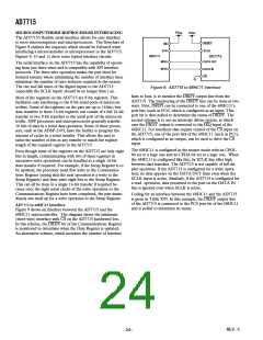
MICROCOMPUTER/MICROPROCESSOR INTERFACING
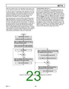
The AD7715’s flexible serial interface allows for easy interface
to most microcomputers and microprocessors. The flowchart of
Figure 8 outlines the sequence which should be followed when
interfacing a microcontroller or microprocessor to the AD7715.
Figures 9, 10 and 11 show some typical interface circuits.
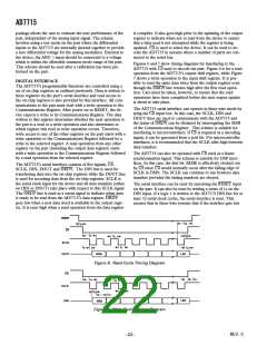
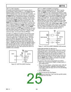
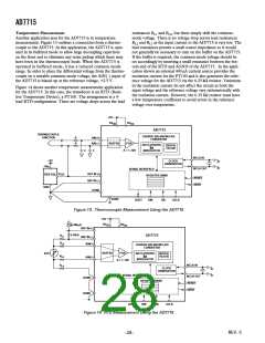
RESET
SS
SCK
SCLK
68HC11
AD7715
MISO
MOSI
DATA OUT
DATA IN
CS
The serial interface on the AD7715 has the capability of operat-
ing from just three wires and is compatible with SPI interface
protocols. The three-wire operation makes the part ideal for
isolated systems where minimizing the number of interface lines
minimizes the number of opto-isolators required in the system.
The rise and fall times of the digital inputs to the AD7715
(especially the SCLK input) should be no longer than 1 µs.
Figure 9. AD7715 to 68HC11 Interface
lines to four, is to monitor the DRDY output line from the
AD7715. The monitoring of the DRDY line can be done in two
ways. First, DRDY can be connected to one of the 68HC11’s
port bits (such as PC0) which is configured as an input. This
port bit is then polled to determine the status of DRDY. The
second scheme is to use an interrupt driven system, in which
case the DRDY output is connected to the IRQ input of the
68HC11. For interfaces that require control of the CS input on
the AD7715, one of the port bits of the 68HC11 (such as PC1),
which is configured as an output, can be used to drive the CS
input.
Most of the registers on the AD7715 are 8-bit registers. This
facilitates easy interfacing to the 8-bit serial ports of microcon-
trollers. Some of the registers on the part are up to 16 bits, but
data transfers to these 16-bit registers can consist of a full 16-bit
transfer or two 8-bit transfers to the serial port of the microcon-
troller. DSP processors and microprocessors generally transfer
16 bits of data in a serial data operation. Some of these proces-
sors, such as the ADSP-2105, have the facility to program the
amount of cycles in a serial transfer. This allows the user to
tailor the number of bits in any transfer to match the register
length of the required register in the AD7715.
The 68HC11 is configured in the master mode with its CPOL
bit set to a logic one and its CPHA bit set to a logic one. When
the 68HC11 is configured like this, its SCLK line idles high
between data transfers. The AD7715 is not capable of full du-
plex operation. If the AD7715 is configured for a write opera-
tion, no data appears on the DATA OUT lines even when the
SCLK input is active. Similarly, if the AD7715 is configured for
a read operation, data presented to the part on the DATA IN
line is ignored even when SCLK is active.
Even though some of the registers on the AD7715 are only eight
bits in length, communicating with two of these registers in
successive write operations can be handled as a single 16-bit
data transfer if required. For example, if the Setup Register is to
be updated, the processor must first write to the Communica-
tions Register (saying that the next operation is a write to the
Setup Register) and then write eight bits to the Setup Register.
This can all be done in a single 16-bit transfer if required be-
cause once the eight serial clocks of the write operation to the
Communications Register have been completed, the part imme-
diately sets itself up for a write operation to the Setup Register.
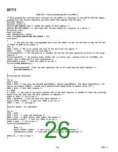
Coding for an interface between the 68HC11 and the AD7715
is given in Table XVI. In this example, the DRDY output line
of the AD7715 is connected to the PC0 port bit of the 68HC11
and is polled to determine its status.
AD7715 to 68HC11 Interface
Figure 9 shows an interface between the AD7715 and the
68HC11 microcontroller. The diagram shows the minimum
(three-wire) interface with CS on the AD7715 hardwired low.
In this scheme, the DRDY bit of the Communications Register
is monitored to determine when the Data Register is updated.
An alternative scheme, which increases the number of interface
REV. C
–24–

 ADI [ ADI ]