AD7715
and gain that can be accommodated by the part is the require-
ment that the positive full-scale calibration limit is ≤ 1.05 ×
VREF/GAIN. This allows the input range to go 5% above the
nominal range. The in-built headroom in the AD7715’s analog
modulator ensures that the part will still operate correctly with a
positive full-scale voltage which is 5% beyond the nominal.
USING THE AD7715
Clocking and Oscillator Circuit
The AD7715 requires a master clock input, which may be an
external CMOS compatible clock signal applied to the MCLK IN
pin with the MCLK OUT pin left unconnected. Alternatively, a
crystal or ceramic resonator of the correct frequency can be
connected between MCLK IN and MCLK OUT in which case
the clock circuit will function as an oscillator, providing the
clock source for the part. The input sampling frequency, the
modulator sampling frequency, the –3 dB frequency, output
update rate and calibration time are all directly related to the
master clock frequency, fCLK IN. Reducing the master clock
frequency by a factor of 2 will halve the above frequencies and
update rate and double the calibration time. The current drawn
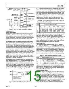
The range of input span in both the unipolar and bipolar modes
has a minimum value of 0.8 × VREF/GAIN and a maximum
value of 2.1 × VREF/GAIN. However, the span (which is the
difference between the bottom of the AD7715’s input range and
the top of its input range) must take into account the limitation
on the positive full-scale voltage. The amount of offset that can
be accommodated depends on whether the unipolar or bipolar
mode is being used. Once again, the offset must take into ac-
count the limitation on the positive full-scale voltage. In unipo-
lar mode, there is considerable flexibility in handling negative
(with respect to AIN(–)) offsets. In both unipolar and bipolar
modes, the range of positive offsets which can be handled by the
part depends on the selected span. Therefore, in determining
the limits for system zero-scale and full-scale calibrations, the
user has to ensure that the offset range plus the span range does
exceed 1.05 × VREF/GAIN. This is best illustrated by looking at
a few examples.
from the DVDD power supply is also directly related to fCLK IN
Reducing fCLK IN by a factor of 2 will halve the DVDD current
but will not affect the current drawn from the AVDD power
supply.
.
Using the part with a crystal or ceramic resonator between the
MCLK IN and MCLK OUT pins generally causes more cur-
rent to be drawn from DVDD than when the part is clocked from
a driven clock signal at the MCLK IN pin. This is because the
on-chip oscillator circuit is active in the case of the crystal or
ceramic resonator. Therefore, the lowest possible current on
the AD7715 is achieved with an externally applied clock at the
MCLK IN pin with MCLK OUT unconnected and unloaded.
If the part is used in unipolar mode with a required span of
0.8 × VREF/GAIN, then the offset range which the system cali-
bration can handle is from –1.05 × VREF/GAIN to +0.25 × VREF
/
GAIN. If the part is used in unipolar mode with a required span of
VREF/GAIN, then the offset range which the system calibration can
handle is from –1.05 × VREF/GAIN to +0.05 × VREF/GAIN. Simi-
larly, if the part is used in unipolar mode and required to re-
move an offset of 0.2 × VREF/GAIN, then the span range which
the system calibration can handle is 0.85 × VREF/GAIN.
The amount of additional current taken by the oscillator de-
pends on a number of factors—first, the larger the value of
capacitor placed on the MCLK IN and MCLK OUT pins, then
the larger the DVDD current consumption on the AD7715. Care
should be taken not to exceed the capacitor values recommended
by the crystal and ceramic resonator manufacturers to avoid
consuming unnecessary DVDD current. Typical values recom-
mended by crystal or ceramic resonator manufacturers are in the
range of 30 pF to 50 pF, and if the capacitor values on MCLK
IN and MCLK OUT are kept in this range, they will not result
in any excessive DVDD current. Another factor that influences
the DVDD current is the effective series resistance (ESR) of the
crystal which appears between the MCLK IN and MCLK OUT
pins of the AD7715. As a general rule, the lower the ESR value
then the lower the current taken by the oscillator circuit.
If the part is used in bipolar mode with a required span of
±0.4 × VREF/GAIN, then the offset range which the system cali-
bration can handle is from –0.65 × VREF/GAIN to +0.65 × VREF
/
GAIN. If the part is used in bipolar mode with a required span
of ±VREF/GAIN, then the offset range which the system calibra-
tion can handle is from –0.05 × VREF/GAIN to +0.05 × VREF
GAIN. Similarly, if the part is used in bipolar mode and required
to remove an offset of ±0.2 × VREF/GAIN, then the span range
/
which the system calibration can handle is ±0.85 × VREF/GAIN.
When operating with a clock frequency of 2.4576 MHz, there is
50 µA difference in the DVDD current between an externally
applied clock and a crystal resonator when operating with a
DVDD of +3 V. With DVDD = +5 V and fCLK IN = 2.4576 MHz,
the typical DVDD current increases by 200 µA for a crystal/
resonator supplied clock versus an externally applied clock. The
ESR values for crystals and resonators at this frequency tend to
be low and as a result there tends to be little difference between
different crystal and resonator types.
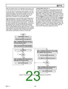
Power-Up and Calibration
On power-up, the AD7715 performs an internal reset that sets
the contents of the internal registers to a known state. There
are default values loaded to all registers after a power-on or
reset. The default values contain nominal calibration coefficients
for the calibration registers. However, to ensure correct calibra-
tion for the device a calibration routine should be performed
after power-up.
The power dissipation and temperature drift of the AD7715 are
low, and no warm-up time is required before the initial calibra-
tion is performed. However, if an external reference is being
used, this reference must have stabilized before calibration is
initiated. Similarly, if the clock source for the part is generated
from a crystal or resonator across the MCLK pins, the start-up
time for the oscillator circuit should elapse before a calibration
is initiated on the part (see below).
When operating with a clock frequency of 1 MHz, the ESR value
for different crystal types varies significantly. As a result, the DVDD
current drain varies across crystal types. When using a crystal
with an ESR of 700 Ω or when using a ceramic resonator, the
increase in the typical DVDD current over an externally-applied
clock is 50 µA with DVDD = +3 V and 175 µA with DVDD
=
+5 V. When using a crystal with an ESR of 3 kΩ, the increase in
the typical DVDD current over an externally applied clock is
100 µA with DVDD = +3 V and 400 µA with DVDD = +5 V.
REV. C
–19–

 ADI [ ADI ]