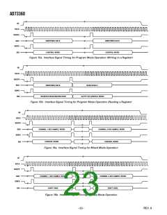
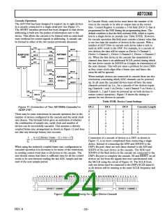
AD73360
Digital Interface
As there are a number of variations of sample rate and clock
speeds that can be used with the AD73360 in a particular appli-
cation, it is important to select the best combination to achieve
the desired performance. High speed serial clocks will read the
data from the AD73360 in a shorter time, giving more time for
processing by at the expense of injecting some digital noise into
the circuit. Digital noise can also be reduced by connecting
resistors (typ <50 Ω) in series with the digital input and output
lines. The noise can be minimized by good grounding and lay-
out. Typically the best performance is achieved by selecting the
slowest sample rate and SCLK frequency for the required appli-
cation as this will produce the least amount of digital noise.
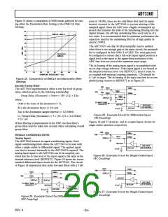
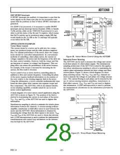
Figure 28 shows combinations of sample rate and SCLK fre-
quency which will allow data to be read from all six channels in
one sample period. These figures correspond to setting DMCLK =
MCLK.
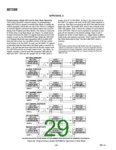
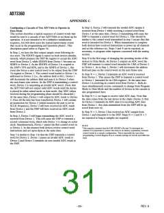
ANALOG GROUND
DIGITAL GROUND
Figure 29. Ground Plane Layout
Avoid running digital lines under the device for they will couple
noise onto the die. The analog ground plane should be allowed
to run under the AD73360 to avoid noise coupling. The power
supply lines to the AD73360 should use as large a trace as pos-
sible to provide low impedance paths and reduce the effects of
glitches on the power supply lines. Fast switching signals such as
clocks should be shielded with digital ground to avoid radiating
noise to other sections of the board, and clock signals should
never be run near the analog inputs. Traces on opposite sides of
the board should run at right angles to each other. This will
reduce the effects of feedthrough through the board. A microstrip
technique is by far the best but is not always possible with a
double-sided board. In this technique, the component side of
the board is dedicated to ground planes while signals are placed
on the other side.
SAMPLE RATE
8KSPS
YES
16KSPS
YES
32KSPS
NO
64KSPS
NO
2MHz
4MHz
8MHz
16MHz
YES
YES
YES
NO
YES
YES
YES
YES
YES
YES
YES
YES
NOTE: SOME COMBINATIONS OF SCLK AND SAMPLE RATE WILL NOT
BE SUFFICIENT TO READ DATA FROM ALL SIX CHANNELS IN THE
ALLOTTED TIME. THESE ARE DEPICTED AS NO.
Figure 28. SCLK and Sample Rates
Grounding and Layout
Good decoupling is important when using high speed devices.
All analog and digital supplies should be decoupled to AGND
and DGND respectively, with 0.1 µF ceramic capacitors in
parallel with 10 µF tantalum capacitors. To achieve the best
from these decoupling capacitors, they should be placed as close
as possible to the device, ideally right up against it. In systems
where a common supply voltage is used to drive both the AVDD
and DVDD of the AD73360, it is recommended that the system’s
AVDD supply be used. This supply should have the recom-
mended analog supply decoupling between the AVDD pins of
the AD73360 and AGND and the recommended digital supply
decoupling capacitors between the DVDD pin and DGND.
Since the analog inputs to the AD73360 are differential, most of
the voltages in the analog modulator are common-mode volt-
ages. The excellent common-mode rejection of the part will
remove common-mode noise on these inputs. The analog and
digital supplies of the AD73360 are independent and separately
pinned out to minimize coupling between analog and digital
sections of the device. The digital filters on the encoder section
will provide rejection of broadband noise on the power supplies,
except at integer multiples of the modulator sampling frequency.
The digital filters also remove noise from the analog inputs
provided the noise source does not saturate the analog modula-
tor. However, because the resolution of the AD73360’s ADC is
high, and the noise levels from the AD73360 are so low, care
must be taken with regard to grounding and layout.
DSP Programming Considerations
This section discusses some aspects of how the serial port of the
DSP should be configured and the implications of whether Rx
and Tx interrupts should be enabled.
The printed circuit board that houses the AD73360 should be
designed so the analog and digital sections are separated and
confined to certain sections of the board. The AD73360 pin
configuration offers a major advantage in that its analog and
digital interfaces are connected on opposite sides of the package.
This facilitates the use of ground planes that can be easily sepa-
rated, as shown in Figure 29. A minimum etch technique is
generally best for ground planes as it gives the best shielding.
Digital and analog ground planes should be joined in only one
place. If this connection is close to the device, it is recommended
to use a ferrite bead inductor as shown in Figure 29.
DSP SPORT Configuration
Following are the key settings of the DSP SPORT required for
the successful operation with the AD73360:
• Configure for external SCLK.
• Serial Word Length = 16 bits.
• Transmit and Receive Frame Syncs required with every word.
• Receive Frame Sync is an input to the DSP.
• Transmit Frame Sync is an:
Input—in Frame Sync Loop-Back Mode
Output—in Nonframe Sync Loop-Back Mode.
• Frame Syncs occur one SCLK cycle before the MSB of the
serial word.
• Frame Syncs are active high.
–26–
REV. B

 ADI [ ADI ]