AD73360
APPENDIX A
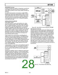
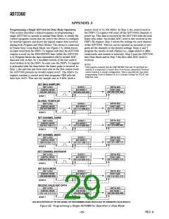
Programming a Single AD73360 for Data Mode Operation
This section describes a typical sequence in programming a
single AD73360 to operate in normal Data Mode. It details the
control (program) words that are sent to the device to configure
its internal registers and shows the typical output data received
during both Program and Data Modes. The device is connected
in Frame Sync Loop-Back Mode (see Figure 13), which forces
an input word from the DSP’s Tx register each time the AD73360
outputs a word via the SDO/SDOFS lines (while the AD73360
is in Program Mode the data transmitted will be invalid ADC
data and will, in fact, be a modified version of the last control
word written in by the DSP). In each case the DSP’s Tx register
is preloaded with the data before the frame pulse is received. In
Step 1, the part has just been reset and on the first output event
the AD73360 presents an invalid output word1. The DSP’s Tx
register contains a control word that programs CRB with the
data byte 0x03. This sets the sample rate at 8 kHz (with a
master clock of 16.384 MHz). In Step 2, the control word in
the DSP’s Tx register will cause all the AD73360s channels to
power up. This data is received by the AD73360 with the next
frame sync pulse. An invalid ADC word is also received at the
DSP’s Rx register. Step 3 selects the settings for each channel
of the AD73360. This set can be repeated as necessary to pro-
gram all the channels to the desired settings. Steps 4 and 5
program the modes of each channel (i.e., single-ended or differ-
ential mode and normal or inverted). Step 6 puts the AD73360
into Data Mode and in Step 7 the first valid ADC word is
received.
NOTE
1This sequence assumes that the DSP SPORT’s Rx and Tx interrupts are
enabled. It is important to ensure there is no latency (separation) between
control words in a cascade configuration. This is especially the case when
programming Control Register B, as it contains settings for SCLK and
DMCLK rates.
SET 8kHz SAMPLING
DSP Tx REG
DEVICE 1
ADC WORD 1*
0000 0000 0000 0000
DSP Rx REG
CONTROL WORD
1000 0001 0000 0011
DON'T CARE
0000 0000 0000 0000
STEP 1
GLOBAL POWER-UP
DSP Rx REG
DSP Tx REG
DEVICE 1
CONTROL WORD
ADC WORD 1*
DON'T CARE
1011 1111 0000 0011
1000 0010 0000 0001
1011 1111 0000 0011
STEP 2
SET CHANNEL GAINS
DSP Rx REG
DSP Tx REG
DEVICE 1
CONTROL WORD
ADC WORD 1*
DON'T CARE
1011 1010 0000 0001
1000 0011 1000 1111
1011 1010 0000 0001
STEP 3
SET CHANNEL MODE
DSP Rx REG
DSP Tx REG
DEVICE 1
CONTROL WORD
ADC WORD 1*
DON'T CARE
1011 1011 1000 1111
1000 0110 0011 1111
1011 1011 1000 1111
STEP 4
SET CHANNEL INVERSION
DSP Rx REG
DSP Tx REG
DEVICE 1
CONTROL WORD
ADC WORD 1*
DON'T CARE
1011 1110 0011 1111
1000 0111 0011 1111
1011 1111 0011 1111
STEP 5
SET DATA MODE
DSP Rx REG
DSP Tx REG
DEVICE 1
CONTROL WORD
ADC WORD 1*
DON'T CARE
1011 1111 0011 1111
1000 0000 0000 0001
1011 1111 0011 1111
STEP 6
RECEIVE VALID ADC DATA
DSP Rx REG
DSP Tx REG
DEVICE 1
CONTROL WORD
ADC WORD 1
ADC WORD 1
1000 0000 0000 0000
0111 1111 1111 1111
1000 0000 0000 0000
STEP 7
*ADC DATA RECEIVED BY THE DSP DURING THE PROGRAMMING PHASE SHOULD NOT BE CONSIDERED VALID RESULTS
Figure 32. Programming a Single AD73360 for Operation in Data Mode
–28–
REV. B

 ADI [ ADI ]