AD73360
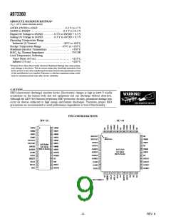
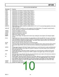
PIN FUNCTION DESCRIPTION
Mnemonic
Function
VINP1
VINN1
VINP2
VINN2
VINP3
VINN3
VINP4
VINN4
VINP5
VINN5
VINP6
VINN6
REFOUT
Analog Input to the Positive Terminal of Input Channel 1.
Analog Input to the Negative Terminal of Input Channel 1.
Analog Input to the Positive Terminal of Input Channel 2.
Analog Input to the Negative Terminal of Input Channel 2.
Analog Input to the Positive Terminal of Input Channel 3.
Analog Input to the Negative Terminal of Input Channel 3.
Analog Input to the Positive Terminal of Input Channel 4.
Analog Input to the Negative Terminal of Input Channel 4.
Analog Input to the Positive Terminal of Input Channel 5.
Analog Input to the Negative Terminal of Input Channel 5.
Analog Input to the Positive Terminal of Input Channel 6.
Analog Input to the Negative Terminal of Input Channel 6.
Buffered Reference Output, which has a nominal value of 1.25 V or 2.5 V, the value being dependent on the status
of Bit 5VEN (CRC:7).
REFCAP
A Bypass Capacitor to AGND2 of 0.1 µF is required for the on-chip reference. The capacitor should be fixed to
this pin. This pin can be overdriven by an external reference if required.
AVDD2
AGND2
DGND
DVDD
RESET
Analog Power Supply Connection.
Analog Ground/Substrate Connection.
Digital Ground/Substrate Connection.
Digital Power Supply Connection.
Active Low Reset Signal. This input resets the entire chip, resetting the control registers and clearing the digital
circuitry.
SCLK
Output Serial Clock whose rate determines the serial transfer rate to/from the AD73360. It is used to clock data or
control information to and from the serial port (SPORT). The frequency of SCLK is equal to the frequency of the
master clock (MCLK) divided by an integer number—this integer number being the product of the external mas-
ter clock rate divider and the serial clock rate divider.
MCLK
SDO
Master Clock Input. MCLK is driven from an external clock signal.
Serial Data Output of the AD73360. Both data and control information may be output on this pin and are clocked
on the positive edge of SCLK. SDO is in three-state when no information is being transmitted and when SE is
low.
SDOFS
SDIFS
Framing Signal Output for SDO Serial Transfers. The frame sync is one bit wide and it is active one SCLK period
before the first bit (MSB) of each output word. SDOFS is referenced to the positive edge of SCLK. SDOFS is in
three-state when SE is low.
Framing Signal Input for SDI Serial Transfers. The frame sync is one bit wide and it is valid one SCLK period
before the first bit (MSB) of each input word. SDIFS is sampled on the negative edge of SCLK and is ignored
when SE is low.
SDI
SE
Serial Data Input of the AD73360. Both data and control information may be input on this pin and are clocked on
the negative edge of SCLK. SDI is ignored when SE is low.
SPORT Enable. Asynchronous input enable pin for the SPORT. When SE is set low by the DSP, the output pins
of the SPORT are three-stated and the input pins are ignored. SCLK is also disabled internally in order to decrease
power dissipation. When SE is brought high, the control and data registers of the SPORT are at their original values
(before SE was brought low); however, the timing counters and other internal registers are at their reset values.
AGND1
AVDD1
Analog Ground Connection.
Analog Power Supply Connection.
REV. B
–9–

 ADI [ ADI ]