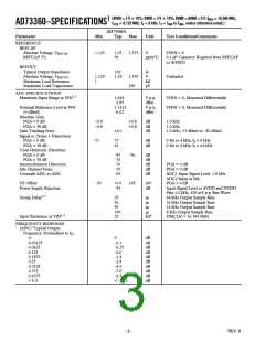
AD73360
(AVDD = 3 V ؎ 10%; DVDD = 3 V ؎ 10%; AGND = DGND = 0 V; TA = TMlN to TMAX, unless otherwise
noted)
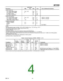
TIMING CHARACTERISTICS
Limit at
Parameter
TA = –40؇C to +85؇C
Unit
Description
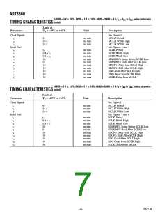
Clock Signals
t1
t2
t3
See Figure 1
MCLK Period
MCLK Width High
MCLK Width Low
61
24.4
24.4
ns min
ns min
ns min
Serial Port
See Figures 3 and 4
t4
t5
t6
t7
t8
t9
t10
t11
t12
t13
t1
ns min
ns min
ns min
ns min
ns min
ns max
ns min
ns min
ns max
ns max
SCLK Period
SCLK Width High
SCLK Width Low
SDI/SDIFS Setup Before SCLK Low
SDI/SDIFS Hold After SCLK Low
SDOFS Delay from SCLK High
SDOFS Hold After SCLK High
SDO Hold After SCLK High
SDO Delay from SCLK High
SCLK Delay from MCLK
0.4 × t1
0.4 × t1
20
0
10
10
10
10
30
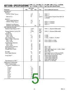
(AVDD = 5 V ؎ 10%; DVDD = 5 V ؎ 10%; AGND = DGND = 0 V; TA = TMlN to TMAX, unless otherwise
noted)
TIMING CHARACTERISTICS
Limit at
Parameter
TA = –40؇C to +85؇C
Unit
Description
Clock Signals
See Figure 1
t1
t2
t3
61
24.4
24.4
ns min
ns min
ns min
MCLK Period
MCLK Width High
MCLK Width Low
Serial Port
See Figures 3 and 4
t4
t5
t6
t7
t8
t9
t10
t11
t12
t13
t1
ns min
ns min
ns min
ns min
ns min
ns max
ns min
ns min
ns max
ns max
SCLK Period
SCLK Width High
SCLK Width Low
SDI/SDIFS Setup Before SCLK Low
SDI/SDIFS Hold After SCLK Low
SDOFS Delay from SCLK High
SDOFS Hold After SCLK High
SDO Hold After SCLK High
SDO Delay from SCLK High
SCLK Delay from MCLK
0.4 × t1
0.4 × t1
20
0
10
10
10
10
30
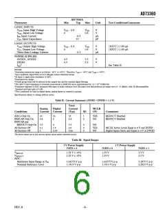
–6–
REV. B

 ADI [ ADI ]