AD73360
AD73360A
Typ
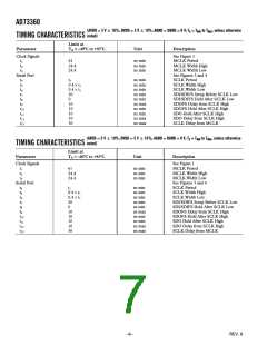
Parameter
Min
Max
Unit
Test Conditions/Comments
LOGIC INPUTS
VINH, Input High Voltage
VDD – 0.8
0
VDD
0.8
V
V
V
INL, Input Low Voltage
IIH, Input Current
CIN, Input Capacitance
–0.5
10
µA
pF
LOGIC OUTPUTS
V
V
OH, Output High Voltage
OL, Output Low Voltage
VDD – 0.4
0
VDD
0.4
V
V
µA
|IOUT| ≤ 100 µA
|IOUT| ≤ 100 µA
Three-State Leakage Current
–0.3
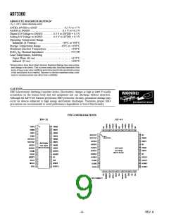
POWER SUPPLIES
AVDD1, AVDD2
DVDD
4.5
4.5
5.5
5.5
V
V
8
IDD
See Table II
NOTES
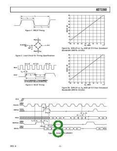
1Operating temperature range is as follows: –40°C to +85°C. Therefore, TMIN = –40°C and TMAX = +85°C.
2Test conditions: Input PGA set for 0 dB gain (unless otherwise noted).
3At input to sigma-delta modulator of ADC.
4Guaranteed by design.
5Overall group delay will be affected by the sample rate and the external digital filtering.
6The ADC’s input impedance is inversely proportional to DMCLK and is approximated by: (4 × 10¹¹)/DMCLK.
7Frequency response of ADC measured with input at audio reference level (the input level that produces an output level of –10 dBm0), with 38 dB preamplifier
bypassed and input gain of 0 dB.
8Test Conditions: no load on digital inputs, analog inputs ac coupled to ground.
Specifications subject to change without notice.
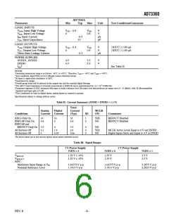
Table II. Current Summary (AVDD = DVDD = 5.5 V)
Total
Analog
Current
Digital
Current
(Typ)
MCLK
ON
Conditions
Current
SE
Comments
ADCs Only On
REFCAP Only On
REFCAP and
16
0.8
16
0
32
0.8
1
0
YES
NO
REFOUT Disabled
REFOUT Disabled
REFOUT Only On 3.5
0
1.9
0.05
3.5
2.0
0.06
0
0
0
NO
YES
NO
All Sections Off
All Sections Off
0.1
0
MCLK Active Levels Equal to 0 V and DVDD
Digital Inputs Static and Equal to 0 V or DVDD
The above values are in mA and are typical values unless otherwise noted.
Table III. Signal Ranges
3 V Power Supply
5 V Power Supply
5VEN = 0
5VEN = 0
5VEN = 1
VREFCAP
VREFOUT
ADC
Maximum Input Range at VIN
Nominal Reference Level
1.25 V 10%
1.25 V 10%
1.25 V
1.25 V
2.5 V
2.5 V
1.64375 V p-p
1.1413 V p-p
1.64375 V p-p
1.1413 V p-p
3.2875 V p-p
2.2823 V p-p
REV. B
–5–

 ADI [ ADI ]