AD5232
Data Sheet
V
DD
USING ADDITIONAL INTERNAL, NONVOLATILE
EEMEM
A
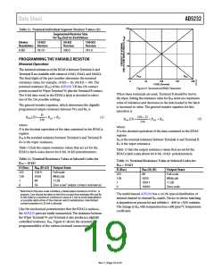
The AD5232 contains additional internal user storage registers
(EEMEM) for saving constants and other 8-bit data. Table 9
provides an address map of the internal nonvolatile storage
registers, which are shown in the functional block diagram as
EEMEM1, EEMEM2, and bytes of USER EEMEM.
W
B
Note the following about EEMEM function:
V
SS
•
RDAC data stored in EEMEM locations are transferred to
their corresponding RDACx register at power-on or when
Command Instruction 1 and Command Instruction 8 are
executed.
USERx refers to internal nonvolatile EEMEM registers that are
available to store and retrieve constants by using Command
Instruction 3 and Command Instruction 9, respectively.
The EEMEM locations are one byte each (eight bits).
Execution of Command Instruction 1 leaves the device in
the read mode power consumption state. When the final
Command Instruction 1 is executed, the user should perform
an NOP (Command Instruction 0) to return the device to
the low power idle state.
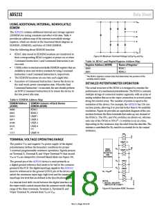
Figure 39. Maximum Terminal Voltages Set by VDD and VSS
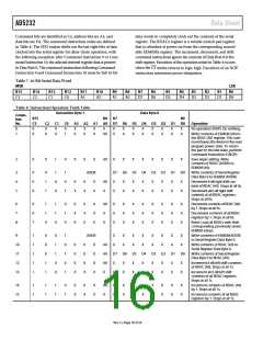
Table 10. RDAC and Digital Register Address Map
Register Address (ADDR)
Name of Register1
RDAC1
•
0000
0001
RDAC2
1
The RDACx registers contain data that determines the position of the
variable resistor wiper.
•
•
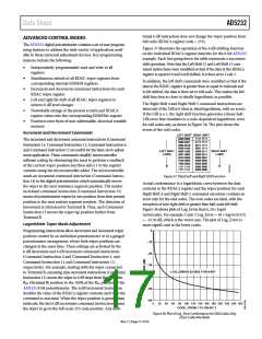
DETAILED POTENTIOMETER OPERATION
The actual structure of the RDACx is designed to emulate the
performance of a mechanical potentiometer. The RDACx contains
multiple strings of connected resistor segments, with an array of
analog switches that act as the wiper connection to several points
along the resistor array. The number of points is equal to the
resolution of the device. For example, the AD5232 has 256 con-
nection points, allowing it to provide better than 0.5% setability
resolution. Figure 40 provides an equivalent diagram of the con-
nections between the three terminals that make up one channel of
the RDACx. The SWA and SWB switches are always on, whereas
only one of the SW(0) to SW(2N–1) switches is on at a time,
depending on the resistance step decoded from the data bits. The
resistance contributed by RW must be accounted for in the output
resistance.
Table 9. EEMEM Address Map
EEMEM Address
(ADDR)
EEMEM Contents of Each Device
EEMEM (ADDR)
0000
0001
0010
0011
0100
0101
***
RDAC1
RDAC2
USER 1
USER 2
USER 3
USER 4
***
USER 14
1111
SW
A
A
TERMINAL VOLTAGE OPERATING RANGE
N
SW(2
–
1)
2)
The positive VDD and negative VSS power supply of the digital
potentiometer defines the boundary conditions for proper
3-terminal programmable resistance operations. Signals present
on Terminal A, Terminal B, and Wiper Terminal W that exceed
W
R
RDAC
WIPER
REGISTER
AND
S
N
SW(2
–
DECODER
VDD or VSS are clamped by a forward biased diode (see Figure 39).
R
R
SW(1)
SW(2)
S
S
The ground pin of the AD5232 device is used primarily as
a digital ground reference that needs to be tied to the common
ground of the PCB. The digital input logic signals to the AD5232
must be referenced to the ground (GND) pin of the device and
satisfy the minimum input logic high level and the maximum
input logic low level that are defined in the Specifications section.
N
R
= R /2
S
AB
SW
B
B
NOTES
1. DIGITAL CIRCUITRY
OMITTED FOR CLARITY
An internal level shift circuit between the digital interface and
the wiper switch control ensures that the common-mode voltage
range of the three terminals, Terminal A, Terminal B, and
Figure 40. Equivalent RDAC Structure
Wiper Terminal W, extends from VSS to VDD
.
Rev. C | Page 18 of 24

 ADI [ ADI ]