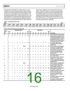
AD5232
Data Sheet
RDAC
10kΩ
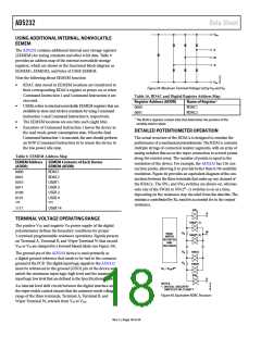
PROGRAMMING THE POTENTIOMETER DIVIDER
A
B
Voltage Output Operation
C
C
B
A
45pF
45pF
C
60pF
The digital potentiometer easily generates an output voltage pro-
portional to the input voltage applied to a given terminal. For
example, connecting Terminal A to 5 V and Terminal B to GND
produces an output voltage at the wiper that can be any value
from 0 V to 5 V. Each LSB of voltage is equal to the voltage
applied across Terminal A to Terminal B, divided by the 2N
position resolution of the potentiometer divider. The general
equation defining the output voltage with respect to ground for
any given input voltage applied to Terminal A to Terminal B is
W
W
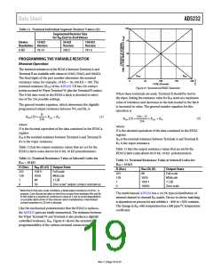
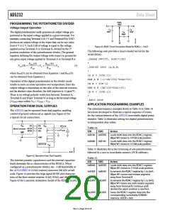
Figure 43. RDAC Circuit Simulation Model for RDACx = 10 kΩ
The following code provides a macro model net list for the
10 kΩ RDAC:
.PARAM DW=255, RDAC=10E3
*
R
WB (D)
RAB
R
RAB
WA (D)
VW (D) =
×VA +
×VB
(3)
.SUBCKT DPOT (A,W,B)
*
where RWB(D) can be obtained from Equation 1 and RWA(D)
can be obtained from Equation 2.
CA A 0 {45E-12}
RAW A W {(1-DW/256)*RDAC+50}
CW W 0 60E-12
RBW W B {DW/256*RDAC+50}
CB B 0 {45E-12}
*
Operation of the digital potentiometer in the divider mode
results in more accurate operation over temperature. Here the
output voltage is dependent on the ratio of the internal resistors,
not the absolute value; therefore, the drift improves to 15 ppm/°C.
There is no voltage polarity restriction between Terminal A,
Terminal B, and Wiper Terminal W as long as the terminal voltage
.ENDS DPOT
(VTERM) stays within VSS < VTERM < VDD
.
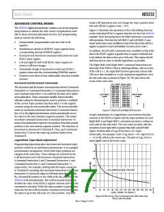
APPLICATION PROGRAMMING EXAMPLES
OPERATION FROM DUAL SUPPLIES
The command sequence examples shown in Table 14 to Table 18
have been developed to illustrate a typical sequence of events
for the various features of the AD5232 nonvolatile digital poten-
tiometer. Table 14 illustrates setting two digital potentiometers
to independent data values.
The AD5232 can be operated from dual supplies, enabling
control of ground-referenced ac signals (see Figure 42 for
a typical circuit connection).
+2.5V
V
SS
CS
V
±2V p-p
±1V p-p
DD
DD
Table 14.
CLK
SDI
SCLK
MOSI
MicroConverter
GND
SDI
SDO
Action
0xB140 0xXXXX
Loads 0x40 data into the RDAC2 register;
Wiper W2 moves to 1/4 full-scale position.
GND
0xB080 0xB140
Loads 0x80 data into the RDAC1 register;
Wiper W1 moves to 1/2 full-scale position.
AD5232
V
SS
Table 15 illustrates the active trimming of one potentiometer,
followed by a save to nonvolatile memory (PCB calibrate).
–2.5V
Figure 42. Operation from Dual Supplies
Table 15.
SDI
The internal parasitic capacitances and the external capacitive
loads dominate the ac characteristics of the RDACs. When
configured as a potentiometer divider, the −3 dB bandwidth of
the AD5232BRU10 (10 kΩ resistor) measures 500 kHz at half
scale. Figure 14 provides the large signal BODE plot character-
istics of the three resistor versions: 10 kΩ, 50 kΩ, and 100 kΩ (see
Figure 43 for a parasitic simulation model of the RDAC circuit).
SDO
Action
0xB040 0xXXXX
Loads 0x40 data into the RDAC1 register;
Wiper W1 moves to 1/4 full-scale position.
Increments the RDAC1 register by 1, to 0x41;
Wiper W1 moves one resistor segment
away from Terminal B.
Increments the RDAC1 register by 1, to 0x42;
Wiper W1 moves one more resistor segment
away from Terminal B. Continue until
desired the wiper position is reached.
Saves the RDAC1 register data into the
corresponding nonvolatile EEMEM1
memory: ADDR = 0x0.
0xE0XX 0xB040
0xE0XX 0xE0XX
0x20XX 0xE0XX
Rev. C | Page 20 of 24

 ADI [ ADI ]