Data Sheet
AD5232
V
DD
SERIAL DATA INTERFACE
The AD5232 contains a 4-wire SPI-compatible digital interface
CS
(SDI, SDO, , and CLK) and uses a 16-bit serial data-word
INPUTS
300Ω
LOGIC
PINS
that is loaded MSB first. The format of the SPI-compatible word
CS
is shown in Table 7. The chip select ( ) pin must be held low
until the complete data-word is loaded into the SDI pin. When
CS
returns high, the serial data-word is decoded according to
AD5232
the instructions in Table 8. The command bits (Cx) control the
operation of the digital potentiometer. The address bits (Ax)
determine which register is activated. The data bits (Dx) are the
values that are loaded into the decoded register. Table 9 provides
an address map of the EEMEM locations. The last command
instruction executed prior to a period of no programming activity
should be the no operation (NOP) command instruction (Com-
mand Instruction 0). This instruction places the internal logic
circuitry in a minimum power dissipation state.
GND
Figure 34. Equivalent ESD Digital Input Protection
V
DD
INPUTS
300Ω
WP
PR
WP
AD5232
VALID
COMMAND
GND
COMMAND
PROCESSOR
AND ADDRESS
DECODE
5V
WP
Figure 35. Equivalent
Input Protection
COUNTER
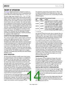
DAISY-CHAINING OPERATION
R
PULL-UP
The SDO pin serves two purposes: it can be used to read back
the contents of the wiper setting and the EEMEM using Command
Instruction 9 and Command Instruction 10 (see Table 8), or it can
be used for daisy-chaining multiple devices.The remaining com-
mand instructions are valid for daisy-chaining multiple devices in
simultaneous operations. Daisy chaining minimizes the number
of port pins required from the controlling IC (see Figure 36).
The SDO pin contains an open-drain N-channel FET that requires
a pull-up resistor if this function is used. As shown in Figure 36,
users must tie the SDO pin of one package to the SDI pin of the
next package. Users may need to increase the clock period because
the pull-up resistor and the capacitive loading at the SDO-to-SDI
interface may require additional time delay between subsequent
packages. If two AD5232s are daisy-chained, 32 bits of data are
required. The first 16 bits go to U2, and the second 16 bits with
the same format go to U1. The 16 bits are formatted to contain
the 4-bit instruction, followed by the 4-bit address, followed by
CLK
SERIAL
REGISTER
SDO
GND
CS
SDI
AD5232
Figure 33. Equivalent Digital Input/Output Logic
The AD5232 has an internal counter that counts a multiple of
16 bits (per frame) for proper operation. For example, the AD5232
works with a 16-bit or 32-bit word, but it cannot work properly
with a 15-bit or 17-bit word. To prevent data from mislocking
(due to noise, for example), the counter resets if the count is not
CS
a multiple of 4 when
register if the count is a multiple of 4. In addition, the AD5232 has
CS
goes high, but the data remains in the
a subtle feature whereby, if
is pulsed without CLK and SDI,
the part repeats the previous command (except during power-
up). As a result, care must be taken to ensure that no excessive
noise exists in the CLK or
number of bits pattern.
CS
the eight bits of data. The
pin should be kept low until all 32 bits
CS
line that may alter the effective
CS
are locked into their respective serial registers. The
pulled high to complete the operation.
pin is then
The equivalent serial data input and output logic is shown in
CS
V
DD
Figure 33. The open-drain SDO is disabled whenever
is logic
high. The SPI interface can be used in two slave modes: CPHA = 1,
CPOL = 1; and CPHA = 0, CPOL = 0. CPHA and CPOL refer
to the control bits that dictate SPI timing in the following micro-
processors and MicroConverter® devices: the ADuC812 and the
ADuC824, the M68HC11, and the MC68HC16R1/916R1. ESD
protection of the digital inputs is shown in Figure 34 and Figure 35.
R
2.2kΩ
P
AD5232
U1
AD5232
U2
SDI
SDO
SDI
SDO
MicroConverter
CS CLK
CLK
CS
Figure 36. Daisy-Chain Configuration Using the SDO
Rev. C | Page 15 of 24

 ADI [ ADI ]