Data Sheet
AD5232
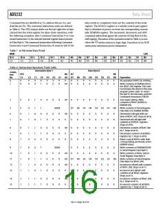
Table 16 illustrates using the left shift-by-one to change circuit
gain in 6 dB steps.
During reliability qualification, Flash/EE memory is cycled
from 0x00 to 0xFF until a first fail is recorded, signifying the
endurance limit of the on-chip Flash/EE memory.
Table 16.
As indicated in the Specifications section, the AD5232 Flash/EE
memory endurance qualification has been carried out in accor-
dance with JEDEC Std. 22, Method A117 over the industrial
temperature range of −40°C to +85°C. The results allow the
specification of a minimum endurance figure over supply and
temperature of 100,000 cycles, with an endurance figure of
700,000 cycles being typical of operation at 25°C.
SDI
SDO
Action
0xC1XX 0xXXXX Moves Wiper W2 to double the present
data value contained in the RDAC2 register
in the direction of Terminal A.
0xC1XX 0xXXXX Moves Wiper W2 to double the present
data value contained in the RDAC2 register
in the direction of Terminal A.
Table 17 illustrates storing additional data in nonvolatile memory.
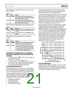
Retention quantifies the ability of the Flash/EE memory to retain
its programmed data over time. Again, the AD5232 has been
qualified in accordance with the formal JEDEC Retention
Lifetime Specification (A117) at a specific junction temperature of
TJ = 55°C. As part of this qualification procedure, the Flash/EE
memory is cycled to its specified endurance limit, as described
previously, before data retention is characterized. This means
that the Flash/EE memory is guaranteed to retain its data for
its full specified retention lifetime every time the Flash/EE
memory is repro-grammed. It should also be noted that
retention lifetime, based on an activation energy of 0.6 eV,
derates with TJ, as shown in Figure 44.
Table 17.
SDI
SDO
Action
0x3280
0xXXXX Stores 0x80 data in spare EEMEM location,
USER1.
0x3340
0xXXXX Stores 0x40 data in spare EEMEM location,
USER2.
Table 18 illustrates reading back data from various memory
locations.
Table 18.
SDI
SDO
Action
300
0x94XX
0xXXXX Prepares data read from USER3 location.
(USER3 is already loaded with 0x80.)
250
200
0x00XX
0xXX80 Instruction 0 (NOP) sends 16-bit word out
of SDO where the last eight bits contain
the contents of USER3 location. The NOP
command ensures that the device returns
to the idle power dissipation state.
ADI TYPICAL PERFORMANCE
150
AT T = 55°C
J
100
50
0
EQUIPMENT CUSTOMER START-UP SEQUENCE
FOR A PCB CALIBRATED UNIT WITH PROTECTED
SETTINGS
WP
1. For the PCB setting, tie
the PCB wiper set position.
2. Set power VDD and VSS with respect to GND.
PR
to GND to prevent changes in
40
50
60
70
80
90
100
110
T
JUNCTION TEMPERATURE (°C)
J
Figure 44. Flash/EE Memory Data Retention
3. As an optional step, strobe the
pin to ensure full power-
on preset of the wiper register with EEMEM contents in
unpredictable supply sequencing environments.
EVALUATION BOARD
Analog Devices, Inc., offers a user-friendly EVAL-AD5232-SDZ
evaluation kit that can be controlled by a personal computer
through a printer port. The driving program is self-contained;
no programming languages or skills are needed.
FLASH/EEMEM RELIABILITY
The Flash/EE memory array on the AD5232 is fully qualified
for two key Flash/EE memory characteristics: namely, Flash/EE
memory cycling endurance and Flash/EE memory data retention.
Endurance quantifies the ability of the Flash/EE memory to be
cycled through many program, read, and erase cycles. In real
terms, a single endurance cycle is composed of four independent,
sequential events. These events are defined as follows:
1. Initial page erase sequence
2. Read/verify sequence
3. Byte program sequence
4. Second read/verify sequence
Rev. C | Page 21 of 24

 ADI [ ADI ]