Setting the Data and MCLK Input Selectors
Power-Up Sequence
The AD1954 contains input selectors for both serial data inputs
and the MCLK input.This allows the AD1954 to select a variety
of input and clock sources with no external hardware required.
These input selectors are controlled by writing to SPI Control
Register 2.
The AD1954 has a built-in power-up sequence that initializes the
contents of the internal RAMs. During this time, the contents
of the internal program boot ROM are copied to the internal
program RAM memory, and likewise, the SPI parameter RAM is
filled with values from its associated boot ROM
.
T
he data memo-
ries are also cleared during this time.
When the data source or MCLK source is changed by writing
to the SPI port, it is possible that a pop or click will occur in the
audio.To prevent this noise, the core should be shut down by
writing a 1 to the halt program bit in Control Register 1.This
initiates a volume ramp-down sequence followed by a shutdown
of the DSP core. Once the core is shut down (which can be veri-
fied by reading Bit 1 from Control Register 1 or by waiting at
least 20 ms after the halt program command is issued), the new
data or MCLK source can be programmed by writing to Control
Register 2.The DSP core can then be restarted by clearing the
halt program bit in Control Register 1.
The boot sequence lasts for 1024 MCLK cycles and starts on the
rising edge of the RESETB pin. Since the boot sequence requires
a stable master clock, the user should avoid writing to or reading
from the SPI registers during this period of time. Note that the
default power-on state of the internal clock mode circuitry is 512
f
S, or about 24 MHz for normal audio sample rates.This mode bypasses all the internal clock doublers and allows the external
master clock to directly operate the DSP core. If the external
master clock is 256
f
S, then the boot sequence will operate at this reduced clock rate and will take slightly longer to complete.
After the boot sequence has finished, the clock modes may be
set via the SPI port. For example, if the external master clock
frequency is 256
f
S clock, the boot sequence would take 1024
256
f
S clock cycles to complete, after which an SPI write could occur to put the AD1954 in 256
f
S mode.
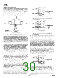
The AD1954 incorporates a feature called data capture. Using
this feature, any node in the signal processing flow may be sent
to either an SPI readable register or a dedicated serial output
pin.This allows the basic functionality of the AD1954 to be
extended to a larger number of channels. Alternatively, it can be
used to monitor and display information about signal levels or
compressor/limiter activity.
The default state of the MCLK input selector is MCLK0. Since
this input selector is controlled using the SPI port, and the SPI port
cannot be written to until the boot sequence is complete, there
must be a stable master clock signal present on the MCLK0 pin at
startup.
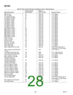
The AD1954 contains four independent data capture registers.
Two of these registers transfer their data to the data capture serial
output (DCSOUT) pin.The serial data format of this pin is the
same as the serial data format used for the main digital inputs,
and the LRCLK and BCLK signals can therefore be used as
frame sync and bit clock signals.This pin is primarily intended
to feed signals to an external DAC or DSP chip to extend the
number of channels that the internal DSP can access
.
T
he other
two registers may be read back over the SPI port and can be used
for a variety of purposes. One example might be to access the dB
output of the internal rms detector to run a front-panel signal
level display. A sample system is shown in Figure 19. For each
of the four data capture registers, a capture count and a register
select must be set.The capture count is a number between 0 and
511 that corresponds to the program step number where the
capture will occur.The register select field programs one of four
registers in the DSP core that will be transferred to the data cap-
ture register when the program counter equals the capture count.
The register select field is decoded as follows:
Setting the Clock Mode
The AD1954 contains a clock doubler circuit that is used to gener-
ate an internal 512
f
S clock when the external clock is 256
f
S.
The clock mode is set by writing to Bit 2 of Control Register 2.
When the clock mode is changed, it is possible that a glitch will
occur on the internal MCLK signal.This may cause the proces-
sor to inadvertently write an incorrect value into the data RAM,
which could cause an audio pop or click sound.To prevent this
the following procedure is recommended:
1. Assert the soft power-down bit (Bit 6 in Control Register 1) to
stop the internal MCLK.
2. Write the desired clock mode into Bit 2 of Control Register 2.
3.
W
a
it
at least 1 ms while the clock doublers settle.
4. De-assert the soft power-down bit.
An alternative procedure is to initiate a soft shutdown of the pro-
cessor core by writing a 1 to the halt program bit in Control
Register 1.This initiates a volume ramp-down sequence followed
by a shutdown of the DSP core. Once the core is shut down (which
can be verified by reading Bit 1 from Control Register 1 or by
waiting at least 20 ms), the new clock mode can be programmed
by writing to Bit 2 of Control Register 2.The DSP core can then
be restarted by clearing the halt program bit in Control Register 1.
00: Multiplier Output (Mult_Out)
01: Output of dB Conversion Block (DB_OUT)
10: Multiplier Data Input (MDI)
11: Multiplier Coefficient Input (MCI)
The capture count and register select bits are set by writing to one
of the four data capture registers at the following SPI addresses:
261: SPI Data Capture Setup Register 1
262: SPI Data Capture Setup Register 2
263: Data Capture Serial Out Setup Register 1
264: Data Capture Serial Out Setup Register 2
REV. A

 ADI [ ADI ]